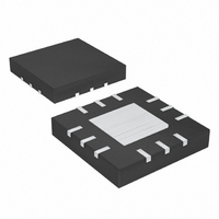
MAX1077ETC+ Maxim Integrated Products, MAX1077ETC+ Datasheet - Page 9

MAX1077ETC+
Manufacturer Part Number
MAX1077ETC+
Description
IC ADC 10BIT 1.5MSPS 12-TQFN
Manufacturer
Maxim Integrated Products
Datasheet
1.MAX1077ETC.pdf
(18 pages)
Specifications of MAX1077ETC+
Number Of Bits
10
Sampling Rate (per Second)
1.5M
Data Interface
MICROWIRE™, QSPI™, Serial, SPI™
Number Of Converters
1
Power Dissipation (max)
22mW
Voltage Supply Source
Analog and Digital
Operating Temperature
-40°C ~ 85°C
Mounting Type
Surface Mount
Package / Case
12-WQFN Exposed Pad
Number Of Adc Inputs
1
Architecture
SAR
Conversion Rate
1500 KSPs
Resolution
10 bit
Input Type
Differential
Interface Type
3-Wire (SPI, QSPI, MICROWIRE)
Voltage Reference
Internal 2.048 V or External
Supply Voltage (max)
3.6 V
Supply Voltage (min)
2.7 V
Maximum Power Dissipation
1349 mW
Maximum Operating Temperature
+ 85 C
Mounting Style
SMD/SMT
Minimum Operating Temperature
- 40 C
Lead Free Status / RoHS Status
Lead free / RoHS Compliant
Figure 3. Functional Diagram
Upon initial power-up, the MAX1077/MAX1079 require a
complete conversion cycle to initialize the internal cali-
bration. Following this initial conversion, the part is ready
for normal operation. This initialization is only required
after a hardware power-up sequence and is not required
after exiting partial or full power-down mode.
To start a conversion, pull CNVST low. At CNVST’s
falling edge, the T/H enters its hold mode and a con-
version is initiated. SCLK runs the conversion, and the
data can then be shifted out serially on DOUT.
Conversion-start and data-read operations are con-
trolled by the CNVST and SCLK digital inputs. Figures
1 and 5 show timing diagrams, which outline the serial-
interface operation.
A CNVST falling edge initiates a conversion sequence:
the T/H stage holds the input voltage, the ADC begins
to convert, and DOUT changes from high impedance
to logic low. SCLK is used to drive the conversion
process, and it shifts data out as each bit of the con-
version is determined.
SCLK begins shifting out the data after the 4th rising
edge of SCLK. DOUT transitions t
SCLK’s rising edge and remains valid 4ns (t
after the next rising edge. The 4th rising clock edge
produces the MSB of the conversion at DOUT, and the
MSB remains valid 4ns after the 5th rising edge. Since
there are 10 data bits, 2 sub-bits (S1 and S0), and 3
leading zeros, at least 16 rising clock edges are need-
Differential, 10-Bit ADCs with Internal Reference
RGND
REF
AIN+
AIN-
T/H
MAX1077
MAX1079
REF 2.048V
1.5Msps, Single-Supply, Low-Power, True-
_______________________________________________________________________________________
Initialization After Power-Up
and Starting a Conversion
10-BIT
ADC
SAR
V
DD
Serial Interface
Timing and Control
LOGIC AND
CONTROL
TIMING
OUTPUT
BUFFER
DOUT
GND
V
L
after each
DHOLD
DOUT
CNVST
SCLK
)
ed to shift out these bits. For continuous operation, pull
CNVST high between the 14th and the 16th SCLK ris-
ing edges. If CNVST stays low after the falling edge of
the 16th SCLK cycle, the DOUT line goes to a high-
impedance state on either CNVST’s rising edge or the
next SCLK’s rising edge.
Power consumption can be reduced significantly by
placing the MAX1077/MAX1079 in either partial power-
down mode or full power-down mode. Partial power-
down mode is ideal for infrequent data sampling and
fast wake-up time applications. Pull CNVST high after
the 3rd SCLK rising edge and before the 14th SCLK
rising edge to enter and stay in partial power-down
mode (see Figure 6). This reduces the supply current
to 2mA. While in partial power-down mode, the refer-
ence remains enabled to allow valid conversions once
the IC is returned to normal mode. Drive CNVST low
and allow at least 14 SCLK cycles to elapse before dri-
ving CNVST high to exit partial power-down mode.
Full power-down mode is ideal for infrequent data sam-
pling and very low supply-current applications. The
MAX1077/MAX1079 have to be in partial power-down
mode to enter full power-down mode. Perform the
SCLK/CNVST sequence described above to enter
Figure 4. Equivalent Input Circuit
AIN+
AIN+
AIN-
AIN-
C
C
C
C
IN+
IN+
IN-
IN-
R
R
R
R
IN+
IN+
IN-
IN-
HOLD/CONVERSION MODE
ACQUISITION MODE
Partial Power-Down and
Full Power-Down Modes
V
V
AZ
AZ
COMP
COMP
CAPACITIVE
CAPACITIVE
CONTROL
CONTROL
LOGIC
LOGIC
DAC
DAC
9


