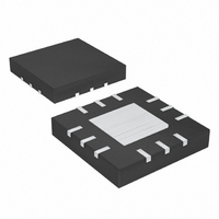
MAX1077ETC+ Maxim Integrated Products, MAX1077ETC+ Datasheet - Page 8

MAX1077ETC+
Manufacturer Part Number
MAX1077ETC+
Description
IC ADC 10BIT 1.5MSPS 12-TQFN
Manufacturer
Maxim Integrated Products
Datasheet
1.MAX1077ETC.pdf
(18 pages)
Specifications of MAX1077ETC+
Number Of Bits
10
Sampling Rate (per Second)
1.5M
Data Interface
MICROWIRE™, QSPI™, Serial, SPI™
Number Of Converters
1
Power Dissipation (max)
22mW
Voltage Supply Source
Analog and Digital
Operating Temperature
-40°C ~ 85°C
Mounting Type
Surface Mount
Package / Case
12-WQFN Exposed Pad
Number Of Adc Inputs
1
Architecture
SAR
Conversion Rate
1500 KSPs
Resolution
10 bit
Input Type
Differential
Interface Type
3-Wire (SPI, QSPI, MICROWIRE)
Voltage Reference
Internal 2.048 V or External
Supply Voltage (max)
3.6 V
Supply Voltage (min)
2.7 V
Maximum Power Dissipation
1349 mW
Maximum Operating Temperature
+ 85 C
Mounting Style
SMD/SMT
Minimum Operating Temperature
- 40 C
Lead Free Status / RoHS Status
Lead free / RoHS Compliant
The MAX1077/MAX1079 use an input T/H and succes-
sive-approximation register (SAR) circuitry to convert
an analog input signal to a digital 10-bit output. The
serial interface requires only three digital lines (SCLK,
CNVST, and DOUT) and provides easy interfacing to
microprocessors (µPs) and DSPs. Figure 3 shows the
simplified internal structure for the MAX1077/MAX1079.
The equivalent circuit of Figure 4 shows the input archi-
tecture of the MAX1077/MAX1079, which is composed of
a T/H, a comparator, and a switched-capacitor digital-to-
analog converter (DAC). The T/H enters its tracking mode
on the 14th SCLK rising edge of the previous conversion.
Upon power-up, the T/H enters its tracking mode immedi-
ately. The positive input capacitor is connected to AIN+.
The negative input capacitor is connected to AIN-. The
T/H enters its hold mode on the falling edge of CNVST
and the difference between the sampled positive and
negative input voltages is converted. The time required
for the T/H to acquire an input signal is determined by
how quickly its input capacitance is charged. If the input
signal’s source impedance is high, the acquisition time
lengthens. The acquisition time, t
1.5Msps, Single-Supply, Low-Power, True-
Differential, 10-Bit ADCs with Internal Reference
8
_______________________________________________________________________________________
5, 11
PIN
10
12
—
1
2
3
4
6
7
8
9
True-Differential Analog Input T/H
CNVST
NAME
RGND
DOUT
SCLK
GND
AIN+
AIN-
N.C.
REF
V
EP
V
DD
L
Detailed Description
Negative Analog Input
Reference Voltage Output. Internal 2.048V reference output. Bypass REF with a 0.01µF capacitor and
a 4.7µF capacitor to RGND.
Reference Ground. Connect RGND to GND.
Positive Analog Supply Voltage (+2.7V to +3.6V). Bypass V
capacitor to GND.
No Connection
Ground. GND is internally connected to EP.
Positive Logic Supply Voltage (1.8V to V
to GND.
Serial Data Output. Data is clocked out on the rising edge of SCLK.
Convert Start. Forcing CNVST high prepares the part for a conversion. Conversion begins on the
falling edge of CNVST. The sampling instant is defined by the falling edge of CNVST.
Serial Clock Input. Clocks data out of the serial interface. SCLK also sets the conversion speed.
Positive Analog Input
Exposed Paddle. EP is internally connected to GND.
ACQ
, is the minimum
time needed for the signal to be acquired. It is calculated
by the following equation:
where R
the input signal.
Note: t
impedance below 12Ω does not significantly affect the
ADC’s AC performance.
The ADC’s input-tracking circuitry has a 15MHz small-
signal bandwidth, making it possible to digitize high-
speed transient events and measure periodic signals
with bandwidths exceeding the ADC’s sampling rate by
using undersampling techniques. To avoid high-fre-
quency signals being aliased into the frequency band
of interest, anti-alias filtering is recommended.
Internal protection diodes that clamp the analog input
to V
from GND - 0.3V to V
inputs must not exceed V
accurate conversions.
DD
). Bypass V
DD
FUNCTION
ACQ
and GND allow the analog input pins to swing
IN
= 200Ω, and RS is the source impedance of
is never less than 125ns, and any source
t
L
ACQ
with a 0.01µF capacitor and a 10µF capacitor
DD
≥ 8 × (RS + R
with a 0.01µF capacitor and a 10µF
DD
Analog Input Protection
+ 0.3V without damage. Both
DD
or be lower than GND for
Pin Description
IN
) × 16pF
Input Bandwidth


