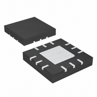
MAX1077ETC+ Maxim Integrated Products, MAX1077ETC+ Datasheet - Page 3

MAX1077ETC+
Manufacturer Part Number
MAX1077ETC+
Description
IC ADC 10BIT 1.5MSPS 12-TQFN
Manufacturer
Maxim Integrated Products
Datasheet
1.MAX1077ETC.pdf
(18 pages)
Specifications of MAX1077ETC+
Number Of Bits
10
Sampling Rate (per Second)
1.5M
Data Interface
MICROWIRE™, QSPI™, Serial, SPI™
Number Of Converters
1
Power Dissipation (max)
22mW
Voltage Supply Source
Analog and Digital
Operating Temperature
-40°C ~ 85°C
Mounting Type
Surface Mount
Package / Case
12-WQFN Exposed Pad
Number Of Adc Inputs
1
Architecture
SAR
Conversion Rate
1500 KSPs
Resolution
10 bit
Input Type
Differential
Interface Type
3-Wire (SPI, QSPI, MICROWIRE)
Voltage Reference
Internal 2.048 V or External
Supply Voltage (max)
3.6 V
Supply Voltage (min)
2.7 V
Maximum Power Dissipation
1349 mW
Maximum Operating Temperature
+ 85 C
Mounting Style
SMD/SMT
Minimum Operating Temperature
- 40 C
Lead Free Status / RoHS Status
Lead free / RoHS Compliant
ELECTRICAL CHARACTERISTICS (continued)
(V
T
Differential, 10-Bit ADCs with Internal Reference
ANALOG INPUTS (AIN+, AIN-)
Differential Input Voltage Range
Absolute Input Voltage Range
DC Leakage Current
Input Capacitance
Input Current (Average)
REFERENCE OUTPUT (REF)
REF Output Voltage Range
Voltage Temperature Coefficient
Load Regulation
Line Regulation
DIGITAL INPUTS (SCLK, CNVST)
Input Voltage Low
Input Voltage High
Input Leakage Current
DIGITAL OUTPUT (DOUT)
Output Load Capacitance
Output Voltage Low
Output Voltage High
Output Leakage Current
POWER REQUIREMENTS
Analog Supply Voltage
Digital Supply Voltage
Analog Supply Current,
Normal Mode
Analog Supply Current,
Partial Power-Down Mode
Analog Supply Current,
Full Power-Down Mode
Digital Supply Current (Note 8)
Positive-Supply Rejection
A
DD
= +25°C.)
= +2.7V to +3.6V, V
PARAMETER
1.5Msps, Single-Supply, Low-Power, True-
_______________________________________________________________________________________
L
= V
DD
, f
SCLK
SYMBOL
C
V
V
PSR
V
VIH
I
I
I
V
VIL
I
= 24MHz, 50% duty cycle, T
V
I
OUT
DD
DD
DD
OL
OH
DD
IL
OL
IN
L
AIN+ - AIN-, MAX1077
AIN+ - AIN-, MAX1079
Per input pin
Time averaged at maximum throughput rate
Static, T
I
I
V
For stated timing performance
I
I
Output high impedance
Static, f
Static, no SCLK
Operational, 1.5Msps
f
No SCLK
f
No SCLK
Operational, full-scale input at 1.5Msps
Static, f
Partial/full power-down mode,
f
Static, no SCLK (all modes)
V
SOURCE
SINK
SINK
SOURCE
SCLK
SCLK
SCLK
DD
DD
= 2.7V to 3.6V, static
= 3V +20% -10%, full-scale input
= 0 to 100µA
= 5mA, V
= 24MHz
= 24MHz
= 24MHz
SCLK
SCLK
A
= 0 to 2mA
= 1mA, V
= +25°C
= 24MHz
= 24MHz
L
CONDITIONS
≥ 1.8V
L
A
≥ 1.8V
= T
MIN
to T
MAX
, unless otherwise noted. Typical values are at
V
-V
0.7 x V
2.038
L
MIN
REF
2.7
1.8
- 0.5V
0
0
/ 2
L
2.048
TYP
0.35
0.25
0.05
±0.2
0.15
±0.2
±50
1.0
0.3
0.3
0.1
0.1
16
75
6
5
7
2
2
1
+V
0.3 x V
2.058
MAX
V
REF
±3.0
V
V
±10
±10
0.4
3.6
0.5
0.3
±1
30
REF
DD
DD
8
7
9
1
1
1
/ 2
L
ppm/°C
mV/mA
UNITS
mV/V
mA
mA
mA
mV
µA
pF
µA
µA
pF
µA
µA
µA
V
V
V
V
V
V
V
V
V
3


