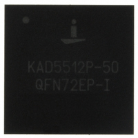
KAD5512P-50Q72 Intersil, KAD5512P-50Q72 Datasheet - Page 18

KAD5512P-50Q72
Manufacturer Part Number
KAD5512P-50Q72
Description
IC ADC 12BIT 500MSPS SGL 72-QFN
Manufacturer
Intersil
Series
FemtoCharge™r
Datasheet
1.KAD5512P-50Q72.pdf
(30 pages)
Specifications of KAD5512P-50Q72
Number Of Bits
12
Sampling Rate (per Second)
500M
Data Interface
Serial, SPI™
Number Of Converters
1
Power Dissipation (max)
460mW
Voltage Supply Source
Single Supply
Operating Temperature
-40°C ~ 85°C
Mounting Type
Surface Mount
Package / Case
72-VFQFN Exposed Pad
For Use With
KDC5512EVAL - DAUGHTER CARD FOR KAD5512KDC5512-50EVAL - DAUGHTER CARD FOR KAD5512
Lead Free Status / RoHS Status
Lead free / RoHS Compliant
In an application where CSB was kept low in sleep mode, the
150µs CSB setup time is not required as the SPI registers are
powered on when CSB is low, the chip power dissipation
increases by ~ 15mW in this case. The 1ms wake-up time
after the write of a ‘001x’ to register 25 still applies. It is
generally recommended to keep CSB high in sleep mode to
avoid any unintentional SPI activity on the ADC.
All digital outputs (Data, CLKOUT and OR) are placed in a
high impedance state during Nap or Sleep. The input clock
should remain running and at a fixed frequency during Nap
or Sleep, and CSB should be high. Recovery time from Nap
mode will increase if the clock is stopped, since the internal
DLL can take up to 52µs to regain lock at 250MSPS.
By default after the device is powered on, the operational
state is controlled by the NAPSLP pin as shown in Table 3.
The power-down mode can also be controlled through the
SPI port, which overrides the NAPSLP pin setting. Details on
this are contained in “Serial Peripheral Interface” on
page 20. This is an indexed function when controlled from
the SPI, but a global function when driven from the pin.
Data Format
Output data can be presented in three formats: two’s
complement, Gray code and offset binary. The data format is
selected via the OUTFMT pin as shown in Table 4.
The data format can also be controlled through the SPI port,
which overrides the OUTFMT pin setting. Details on this are
contained in “Serial Peripheral Interface” on page 20.
Offset binary coding maps the most negative input voltage to
code 0x000 (all zeros) and the most positive input to 0xFFF
(all ones). Two’s complement coding simply complements
the MSB of the offset binary representation.
When calculating Gray code the MSB is unchanged. The
remaining bits are computed as the XOR of the current bit
position and the next most significant bit. Figure 30 shows
this operation.
NAPSLP PIN
OUTFMT PIN
AVSS
AVDD
AVSS
AVDD
Float
Float
TABLE 4. OUTFMT PIN SETTINGS
TABLE 3. NAPSLP PIN SETTINGS
18
Two’s Complement
Offset Binary
Gray Code
Normal
MODE
MODE
Sleep
Nap
KAD5512P-50
Converting back to offset binary from Gray code must be
done recursively, using the result of each bit for the next
lower bit as shown in Figure 31.
Mapping of the input voltage to the various data formats is
shown in Table 5.
–Full Scale 000 00 000 00 00 100 00 000 00 00 000 00 000 00 00
–Full Scale
+Full Scale
+Full Scale 111 11 111 11 11
VOLTAGE OFFSET BINARY
Mid–Scale 100 00 000 00 00 000 00 000 00 00 110 00 000 00 00
+ 1LSB
– 1LSB
INPUT
TABLE 5. INPUT VOLTAGE TO OUTPUT CODE MAPPING
GRAY CODE
FIGURE 30. BINARY TO GRAY CODE CONVERSION
FIGURE 31. GRAY CODE TO BINARY CONVERSION
GRAY CODE
BINARY
BINARY
000 00 000 00 01 100 00 000 00 01 000 00 000 00 01
111 11 111 11 10
11
11
11
11
10
10
10
10
011 11 111 11 10 100 00 000 00 01
011 11 111 111 1 100 00 000 00 00
COMPLEMENT
9
9
TWO’S
9
9
• • • •
• • • •
• • • •
• • • •
• • • •
• • • •
• • • •
GRAY CODE
October 9, 2009
1
1
1
1
FN6805.3
0
0
0
0


