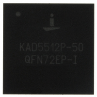
KAD5512P-50Q72 Intersil, KAD5512P-50Q72 Datasheet - Page 14

KAD5512P-50Q72
Manufacturer Part Number
KAD5512P-50Q72
Description
IC ADC 12BIT 500MSPS SGL 72-QFN
Manufacturer
Intersil
Series
FemtoCharge™r
Datasheet
1.KAD5512P-50Q72.pdf
(30 pages)
Specifications of KAD5512P-50Q72
Number Of Bits
12
Sampling Rate (per Second)
500M
Data Interface
Serial, SPI™
Number Of Converters
1
Power Dissipation (max)
460mW
Voltage Supply Source
Single Supply
Operating Temperature
-40°C ~ 85°C
Mounting Type
Surface Mount
Package / Case
72-VFQFN Exposed Pad
For Use With
KDC5512EVAL - DAUGHTER CARD FOR KAD5512KDC5512-50EVAL - DAUGHTER CARD FOR KAD5512
Lead Free Status / RoHS Status
Lead free / RoHS Compliant
Theory of Operation
Functional Description
The KAD5512P-50 is based upon a 12-bit, 250MSPS A/D
converter core that utilizes a pipelined successive
approximation architecture (Figure 20). The input voltage is
captured by a Sample-Hold Amplifier (SHA) and converted to
a unit of charge. Proprietary charge-domain techniques are
used to successively compare the input to a series of
reference charges. Decisions made during the successive
approximation operations determine the digital code for each
input value. The converter pipeline requires twelve samples to
produce a result. Digital error correction is also applied,
resulting in a total latency of fifteen clock cycles. This is
evident to the user as a latency between the start of a
conversion and the data being available on the digital outputs.
The device contains two units A/D converters with carefully
matched transfer characteristics. The cores are clocked on
alternate clock edges, resulting in a doubling of the sample
rate. The gain, offset and skew errors between the two unit
ADCs can be adjusted via the SPI port to minimize spurs
associated with the interleaving process.
Time–interleaved ADC systems can exhibit non–ideal
artifacts in the frequency domain if the individual unit ADC
characteristics are not well matched. Gain, offset and timing
skew mismatches are of primary concern.
Main mismatch results in fundamental image spurs at
f
sampling instances for the two unit ADCs, will result in spurs
in the same locations. Offset mismatches create spurs at DC
and multiples of f
NYQUIST
± f
IN
. Mismatches in timing skew, which shift the
INP
INN
NYQUIST
1.25V
.
14
+
–
SHA
FIGURE 20. ADC CORE BLOCK DIAGRAM
2.5-BIT
FLASH
KAD5512P-50
1.5-BIT/STAGE
6-STAGE
The design of the KAD5512P-50 minimizes the effect of
process, voltage and temperature variations on the matching
characteristics of the two unit ADCs. The gain and offset of
the two unit ADCs are adjusted after power-on calibration to
minimize the mismatch between the channels. All calibration
is performed using internally generated signals, with the
analog input signal disconnected from the sample and hold
amplifier (SHA).
The KAD5512P-50 does not have the ability to adjust timing
skew mismatches as part of the internal calibration sequence.
Clock routing to each unit ADC is carefully matched, however
some timing skew will exist that may result in a detectable
fundamental image spur at f
Power-On Calibration
As mentioned previously, the cores perform a self-calibration
at start-up. An internal power-on-reset (POR) circuit detects
the supply voltage ramps and initiates the calibration when
the analog and digital supply voltages are above a threshold.
The following conditions must be adhered to for the
power-on calibration to execute successfully:
• A frequency-stable conversion clock must be applied to
• DNC pins (especially 3, 4 and 18) must not be pulled up or
• SDO (pin 66) must be high
• RESETN (pin 25) must begin low
• SPI communications must not be attempted
A user-initiated reset can subsequently be invoked in the
event that the above conditions cannot be met at power-up.
the CLKP/CLKN pins
down
LVDS/LVCMOS
CORRECTION
GENERATION
OUTPUTS
DIGITAL
CLOCK
ERROR
1-BIT/STAGE
3-STAGE
NYQUIST
FLASH
3-BIT
± f
IN
.
October 9, 2009
FN6805.3


