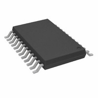
AD7190BRUZ Analog Devices Inc, AD7190BRUZ Datasheet - Page 24

AD7190BRUZ
Manufacturer Part Number
AD7190BRUZ
Description
IC ADC 2CH 24BIT W/PGA 24TSSOP
Manufacturer
Analog Devices Inc
Datasheet
1.AD7190BRUZ.pdf
(40 pages)
Specifications of AD7190BRUZ
Data Interface
DSP, MICROWIRE™, QSPI™, Serial, SPI™
Design Resources
Precision Weigh Scale Design Using AD7190 with Internal PGA (CN0102)
Number Of Bits
24
Sampling Rate (per Second)
4.8k
Number Of Converters
1
Voltage Supply Source
Analog and Digital
Operating Temperature
-40°C ~ 105°C
Mounting Type
Surface Mount
Package / Case
24-TSSOP (0.173", 4.40mm Width)
Resolution (bits)
24bit
Sampling Rate
4.8kSPS
Input Channel Type
Pseudo Differential
Supply Voltage Range - Analog
4.75V To 5.25V
Lead Free Status / RoHS Status
Lead free / RoHS Compliant
Available stocks
Company
Part Number
Manufacturer
Quantity
Price
Company:
Part Number:
AD7190BRUZ
Manufacturer:
ADI
Quantity:
1 000
Part Number:
AD7190BRUZ
Manufacturer:
ADI/亚德诺
Quantity:
20 000
Company:
Part Number:
AD7190BRUZ-REEL
Manufacturer:
ADI
Quantity:
1 000
Part Number:
AD7190BRUZ-REEL
Manufacturer:
ADI/亚德诺
Quantity:
20 000
AD7190
Table 20. Channel Selection
Channel Enable Bits in the Configuration Register
CH7
1
DATA REGISTER
(RS2, RS1, RS0 = 0, 1, 1; Power-On/Reset = 0x000000)
The conversion result from the ADC is stored in this data
register. This is a read-only, 24-bit register. On completion of a
read operation from this register, the RDY pin/bit is set. When
the DAT_STA bit in the mode register is set to 1, the contents of
the status register are appended to each 24-bit conversion. This
is advisable when several analog input channels are enabled
because the three LSBs of the status register (CHD2 to CHD0)
identify the channel from which the conversion originated.
CH6
1
CH5
1
CH4
1
CH3
1
CH2
1
CH1
1
CH0
1
Rev. B | Page 24 of 40
Channel Enabled
Positive Input
AIN(+)
AIN1
AIN3
AIN2
AIN1
AIN2
AIN3
AIN4
Temperature sensor
ID REGISTER
RS2, RS1, RS0 = 1, 0, 0; Power-On/Reset = 0xX4
The identification number for the AD7190 is stored in the ID
register. This is a read-only register.
GPOCON REGISTER
(RS2, RS1, RS0 = 1, 0, 1; Power-On/Reset = 0x00)
The GPOCON register is an 8-bit register from which data can
be read or to which data can be written. This register is used to
enable the general-purpose digital outputs.
Table 21 outlines the bit designations for the GPOCON register.
GP0 through GP7 indicate the bit locations. GP denotes that the
bits are in the GPOCON register. GP7 denotes the first bit of
the data stream. The number in parentheses indicates the
power-on/reset default status of that bit.
AIN2
AIN4
AIN2
AINCOM
AINCOM
AINCOM
AINCOM
Negative Input
AIN(−)
Status Register
Bits CHD[2:0]
000
001
010
011
100
101
110
111
Calibration
Register Pair
0
1
None
0
0
1
2
3


