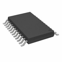
AD7190BRUZ Analog Devices Inc, AD7190BRUZ Datasheet - Page 10

AD7190BRUZ
Manufacturer Part Number
AD7190BRUZ
Description
IC ADC 2CH 24BIT W/PGA 24TSSOP
Manufacturer
Analog Devices Inc
Datasheet
1.AD7190BRUZ.pdf
(40 pages)
Specifications of AD7190BRUZ
Data Interface
DSP, MICROWIRE™, QSPI™, Serial, SPI™
Design Resources
Precision Weigh Scale Design Using AD7190 with Internal PGA (CN0102)
Number Of Bits
24
Sampling Rate (per Second)
4.8k
Number Of Converters
1
Voltage Supply Source
Analog and Digital
Operating Temperature
-40°C ~ 105°C
Mounting Type
Surface Mount
Package / Case
24-TSSOP (0.173", 4.40mm Width)
Resolution (bits)
24bit
Sampling Rate
4.8kSPS
Input Channel Type
Pseudo Differential
Supply Voltage Range - Analog
4.75V To 5.25V
Lead Free Status / RoHS Status
Lead free / RoHS Compliant
Available stocks
Company
Part Number
Manufacturer
Quantity
Price
Company:
Part Number:
AD7190BRUZ
Manufacturer:
ADI
Quantity:
1 000
Part Number:
AD7190BRUZ
Manufacturer:
ADI/亚德诺
Quantity:
20 000
Company:
Part Number:
AD7190BRUZ-REEL
Manufacturer:
ADI
Quantity:
1 000
Part Number:
AD7190BRUZ-REEL
Manufacturer:
ADI/亚德诺
Quantity:
20 000
AD7190
PIN CONFIGURATION AND FUNCTION DESCRIPTIONS
Table 5. Pin Function Descriptions
Pin No.
1
2
3
4
5
6
7
8
9
10
11
12
Mnemonic
MCLK1
MCLK2
SCLK
CS
P3
P2
P1/REFIN2(+)
P0/REFIN2(−)
NC
AINCOM
AIN1
AIN2
Description
When the master clock for the device is provided externally by a crystal, the crystal is connected between
MCLK1 and MCLK2.
Master Clock Signal for the Device. The AD7190 has an internal 4.92 MHz clock. This internal clock can be
made available on the MCLK2 pin. The clock for the AD7190 can be provided externally also in the form of
a crystal or external clock. A crystal can be tied across the MCLK1 and MCLK2 pins. Alternatively, the
MCLK2 pin can be driven with a CMOS-compatible clock and the MCLK1 pin left unconnected.
Serial Clock Input. This serial clock input is for data transfers to and from the ADC. The SCLK has a Schmitt-
triggered input, making the interface suitable for opto-isolated applications. The serial clock can be
continuous with all data transmitted in a continuous train of pulses. Alternatively, it can be a noncon-
tinuous clock with the information transmitted to or from the ADC in smaller batches of data.
Chip Select Input. This is an active low logic input used to select the ADC. CS can be used to select the ADC
in systems with more than one device on the serial bus or as a frame synchronization signal in
communicating with the device. CS can be hardwired low, allowing the ADC to operate in 3-wire mode
with SCLK, DIN, and DOUT used to interface with the device.
Digital Output Pin. This pin can function as a general-purpose output bit referenced between AV
Digital Output Pin. This pin can function as a general-purpose output bit referenced between AV
Digital Output Pin/Positive Reference Input. This pin functions as a general-purpose output bit referenced
between AV
applied between REFIN2(+) and REFIN2(−). REFIN2(+) can lie anywhere between AV
nominal reference voltage, (REFIN2(+) − REFIN2(−)), is AV
1 V to AV
Digital Output Pin/Negative Reference Input. This pin functions as a general-purpose output bit referenced
between AV
anywhere between AGND and AV
No Connect. This pin should be tied to AGND.
Analog Input AIN1 to Analog Input AIN4 are referenced to this input when configured for pseudo
differential operation.
Analog Input. It can be configured as the positive input of a fully differential input pair when used with
AIN2 or as a pseudo differential input when used with AINCOM.
Analog Input. It can be configured as the negative input of a fully differential input pair when used with
AIN1 or as a pseudo differential input when used with AINCOM.
DD
.
DD
DD
and AGND. When REFSEL = 1, this pin functions as REFIN2(+). An external reference can be
and AGND. When REFSEL = 1, this pin functions as REFIN2(−). This reference input can lie
P1/REFIN2(+)
P0/REFIN2(–)
AINCOM
MCLK1
MCLK2
SCLK
AIN1
AIN2
NC
CS
P3
P2
Figure 5. Pin Configuration
10
12
11
1
2
3
4
5
6
7
8
9
Rev. B | Page 10 of 40
NC = NO CONNECT
(Not to Scale)
AD7190
TOP VIEW
DD
− 1 V.
24
22
20
19
18
17
16
15
14
13
23
21
DIN
DOUT/RDY
SYNC
DV
AV
DGND
AGND
BPDSW
REFIN1(–)
REFIN1(+)
AIN4
AIN3
DD
DD
DD
, but the part functions with a reference from
DD
and AGND + 1 V. The
DD
DD
and AGND.
and AGND.


