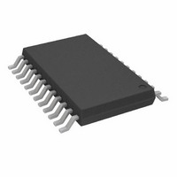
AD7190BRUZ Analog Devices Inc, AD7190BRUZ Datasheet - Page 19

AD7190BRUZ
Manufacturer Part Number
AD7190BRUZ
Description
IC ADC 2CH 24BIT W/PGA 24TSSOP
Manufacturer
Analog Devices Inc
Datasheet
1.AD7190BRUZ.pdf
(40 pages)
Specifications of AD7190BRUZ
Data Interface
DSP, MICROWIRE™, QSPI™, Serial, SPI™
Design Resources
Precision Weigh Scale Design Using AD7190 with Internal PGA (CN0102)
Number Of Bits
24
Sampling Rate (per Second)
4.8k
Number Of Converters
1
Voltage Supply Source
Analog and Digital
Operating Temperature
-40°C ~ 105°C
Mounting Type
Surface Mount
Package / Case
24-TSSOP (0.173", 4.40mm Width)
Resolution (bits)
24bit
Sampling Rate
4.8kSPS
Input Channel Type
Pseudo Differential
Supply Voltage Range - Analog
4.75V To 5.25V
Lead Free Status / RoHS Status
Lead free / RoHS Compliant
Available stocks
Company
Part Number
Manufacturer
Quantity
Price
Company:
Part Number:
AD7190BRUZ
Manufacturer:
ADI
Quantity:
1 000
Part Number:
AD7190BRUZ
Manufacturer:
ADI/亚德诺
Quantity:
20 000
Company:
Part Number:
AD7190BRUZ-REEL
Manufacturer:
ADI
Quantity:
1 000
Part Number:
AD7190BRUZ-REEL
Manufacturer:
ADI/亚德诺
Quantity:
20 000
ON-CHIP REGISTERS
The ADC is controlled and configured via a number of on-chip
registers, which are described in the following sections. In the
descriptions, set implies a Logic 1 state and cleared implies a
Logic 0 state, unless otherwise noted.
COMMUNICATIONS REGISTER
(RS2, RS1, RS0 = 0, 0, 0)
The communications register is an 8-bit write-only register. All
communications to the part must start with a write operation to
the communications register. The data written to the communi-
cations register determines whether the next operation is a read
or write operation and in which register this operation takes
place. For read or write operations, when the subsequent read
or write operation to the selected register is complete, the
CR7
WEN(0)
Table 14. Communications Register Bit Designations
Bit Location
CR7
CR6
CR5 to CR3
CR2
CR1 to CR0
Table 15. Register Selection
RS2
0
0
0
0
0
1
1
1
1
RS1
0
0
0
1
1
0
0
1
1
CR6
R/W(0)
Bit Name
WEN
R/W
RS2 to RS0
CREAD
RS0
0
0
1
0
1
0
1
0
1
Register
Communications register during a write operation
Status register during a read operation
Mode register
Configuration register
Data register/data register plus status information
ID register
GPOCON register
Offset register
Full-scale register
Description
Write enable bit. A 0 must be written to this bit for a write to the communications register to occur. If a 1 is
the first bit written, the part does not clock on to subsequent bits in the register. It stays at this bit location
until a 0 is written to this bit. After a 0 is written to the WEN bit, the next seven bits are loaded to the
communications register.
A 0 in this bit location indicates that the next operation is a write to a specified register. A 1 in this position
indicates that the next operation is a read from the designated register.
Register address bits. These address bits are used to select which registers of the ADC are selected during
the serial interface communication. See Table 15.
Continuous read of the data register. When this bit is set to 1 (and the data register is selected), the serial
interface is configured so that the data register can be continuously read; that is, the contents of the data
register are automatically placed on the DOUT pin when the SCLK pulses are applied after the RDY pin
goes low to indicate that a conversion is complete. The communications register does not have to be
written to for subsequent data reads. To enable continuous read, the instruction 01011100 must be written
to the communications register. To disable continuous read, the instruction 01011000 must be written to
the communications register while the RDY pin is low. While continuous read is enabled, the ADC monitors
activity on the DIN line so that it can receive the instruction to disable continuous read. Additionally, a reset
occurs if 40 consecutive 1s are seen on DIN. Therefore, DIN should be held low until an instruction is to be
written to the device.
These bits must be programmed to Logic 0 for correct operation.
CR5
RS2(0)
CR4
RS1(0)
Rev. B | Page 19 of 40
CR3
RS0(0)
interface returns to where it expects a write operation to
the communications register. This is the default state of the
interface and, on power-up or after a reset, the ADC is in this
default state waiting for a write operation to the communi-
cations register. In situations where the interface sequence is
lost, a write operation of at least 40 serial clock cycles with DIN
high returns the ADC to this default state by resetting the entire
part. Table 14 outlines the bit designations for the
communications register. CR0 through CR7 indicate the bit
locations, CR denoting that the bits are in the communications
register. CR7 denotes the first bit of the data stream. The
number in parentheses indicates the power-on/reset default
status of that bit.
CR2
CREAD(0)
CR1
0(0)
Register Size
8 bits
8 bits
24 bits
24 bits
24 bits/32 bits
8 bits
8 bits
24 bits
24 bits
CR0
0(0)
AD7190


