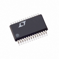
LTC2408CG#PBF Linear Technology, LTC2408CG#PBF Datasheet - Page 32

LTC2408CG#PBF
Manufacturer Part Number
LTC2408CG#PBF
Description
IC A/D CONV 24BIT 8-CHAN 28-SSOP
Manufacturer
Linear Technology
Datasheet
1.LTC2408CGPBF.pdf
(36 pages)
Specifications of LTC2408CG#PBF
Number Of Bits
24
Sampling Rate (per Second)
7.5
Data Interface
MICROWIRE™, Serial, SPI™
Number Of Converters
1
Power Dissipation (max)
1mW
Voltage Supply Source
Single Supply
Operating Temperature
0°C ~ 70°C
Mounting Type
Surface Mount
Package / Case
28-SSOP (0.200", 5.30mm Width)
Number Of Elements
1
Resolution
24Bit
Architecture
Delta-Sigma
Sample Rate
0.008KSPS
Input Polarity
Unipolar
Input Type
Voltage
Rated Input Volt
6.188V
Differential Input
No
Power Supply Requirement
Single
Single Supply Voltage (typ)
3.3/5V
Single Supply Voltage (min)
2.7V
Single Supply Voltage (max)
5.5V
Dual Supply Voltage (typ)
Not RequiredV
Dual Supply Voltage (min)
Not RequiredV
Dual Supply Voltage (max)
Not RequiredV
Differential Linearity Error
1LSB(Typ)
Integral Nonlinearity Error
15ppm of Vref
Operating Temp Range
0C to 70C
Operating Temperature Classification
Commercial
Mounting
Surface Mount
Pin Count
28
Package Type
SSOP
Input Signal Type
Single-Ended
Lead Free Status / RoHS Status
Lead free / RoHS Compliant
Available stocks
Company
Part Number
Manufacturer
Quantity
Price
APPLICATIONS
LTC2404/LTC2408
*****************************************************************************
*
* This example program loads multiplexer channels selection data into
* either the LTC2408’s internal MUX or an external LTC1391 MUX. It then
* transfers the LTC2408’s 32-bit output conversion result to four
* consecutive 8-bit memory locations.
*
*
*****************************************************************************
*
***************************************
* 68HC11 register definitions
***************************************
*
PORTD
*
DDRD
SPCR
*
SPSR
*
SPDR
*
* RAM variables to hold the LTC2408’s 32 conversion result
*
DIN1
DIN2
DIN3
DIN4
MUX
*
***************************************
* Start GETDATA Routine
***************************************
*
INIT1
*
*
* DDRD’s bit 5 is a 1 so that port D’s SS* pin is a general output
*
*
*
*
GETDATA PSHX
*
*
***************************************
* The next routine sends data to the
* LTC2408 an sets its MUX channel
***************************************
*
32
EQU
EQU
EQU
EQU
EQU
EQU
EQU
ORG
LDAA
STAA
LDAA
STAA
LDAA
STAA
PSHY
PSHA
LDX
LDY
LDAA
TAB
SUBA
BLE
TBA
ORAA
BRA
EQU
EQU
EQU
$1008
$1009
$1028
$1029
$102A
$00
$01
$02
$03
$04
$C000
#$2F
PORTD
#$38
DDRD
#$50
SPCR
#$0
#$1000
MUX
#$07
ENLWMX If it is, branch to enable the LTC2408’s internal MUX
#$80
MUXSPI
U
Port D data register
“ - , - , SS* ,CSK ;MOSI,MISO,TxD ,RxD “
Port D data direction register
SPI control register
“SPIE,SPE ,DWOM,MSTR;SPOL,CPHA,SPR1,SPR0”
SPI status register
“SPIF,WCOL, - ,MODF; - , - , - , - “
SPI data register; Read-Buffer; Write-Shifter
This memory location holds the LTC2408’s bits 31 - 24
This memory location holds the LTC2408’s bits 23 - 16
This memory location holds the LTC2408’s bits 15 - 08
This memory location holds the LTC2408’s bits 07 - 00
This memory location holds the MUX address data
Program start location
-,-,1,0;1,1,1,1
-, -, SS*-Hi, SCK-Lo, MOSI-Hi, MISO-Hi, X, X
Keeps SS* a logic high when DDRD, bit 5 is set
-,-,1,1;1,0,0,0
SS* , SCK, MOSI are configured as Outputs
MISO, TxD, RxD are configured as Inputs
The SPI is configured as Master, CPHA = 0, CPOL = 0
and the clock rate is E/2
(This assumes an E-Clock frequency of 4MHz. For higher
E-Clock frequencies, change the above value of $50 to a
value that ensures the SCK frequency is 2MHz or less.)
The X register is used as a pointer to the memory
locations that hold the conversion data
Retrieve MUX address
Save contents of Accum. A
Is the MUX address in the low nibble
Restore contents of Accum. A
Enable the LTC1391 external MUX
Go to SPI transfer2400
INFORMATION
U
*
*
*
*
W
U
*
*
*
*
*


