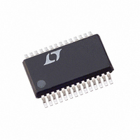
LTC2408CG#PBF Linear Technology, LTC2408CG#PBF Datasheet - Page 29

LTC2408CG#PBF
Manufacturer Part Number
LTC2408CG#PBF
Description
IC A/D CONV 24BIT 8-CHAN 28-SSOP
Manufacturer
Linear Technology
Datasheet
1.LTC2408CGPBF.pdf
(36 pages)
Specifications of LTC2408CG#PBF
Number Of Bits
24
Sampling Rate (per Second)
7.5
Data Interface
MICROWIRE™, Serial, SPI™
Number Of Converters
1
Power Dissipation (max)
1mW
Voltage Supply Source
Single Supply
Operating Temperature
0°C ~ 70°C
Mounting Type
Surface Mount
Package / Case
28-SSOP (0.200", 5.30mm Width)
Number Of Elements
1
Resolution
24Bit
Architecture
Delta-Sigma
Sample Rate
0.008KSPS
Input Polarity
Unipolar
Input Type
Voltage
Rated Input Volt
6.188V
Differential Input
No
Power Supply Requirement
Single
Single Supply Voltage (typ)
3.3/5V
Single Supply Voltage (min)
2.7V
Single Supply Voltage (max)
5.5V
Dual Supply Voltage (typ)
Not RequiredV
Dual Supply Voltage (min)
Not RequiredV
Dual Supply Voltage (max)
Not RequiredV
Differential Linearity Error
1LSB(Typ)
Integral Nonlinearity Error
15ppm of Vref
Operating Temp Range
0C to 70C
Operating Temperature Classification
Commercial
Mounting
Surface Mount
Pin Count
28
Package Type
SSOP
Input Signal Type
Single-Ended
Lead Free Status / RoHS Status
Lead free / RoHS Compliant
Available stocks
Company
Part Number
Manufacturer
Quantity
Price
APPLICATIONS
noise bandwidth of the system to 6Hz. The noise band-
width of the LTC2408 without any input bandwidth lim-
iting is approximately 150Hz. A roll-off at 1500Hz
eliminates all higher order images of the base bandwidth
of 6Hz. In the example shown, the optional bandwidth-
limiting filter has a – 3dB point at 1450Hz. This filter can be
inserted after the multiplexer provided that higher source
impedance prior to the multiplexer does not reduce the
– 3dB frequency, extending settling time, and resulting in
charge sharing between samples. The settling time of this
filter to 20+ bits of accuracy is less than 2ms. In the pres-
ence of external wideband noise, this filter reduces the
apparent noise by a factor of 5. Note that the noise band-
width for noise developed in the amplifier is 150Hz. In the
example shown, the gain of the amplifier is set to 40, the
point at which amplifier noise gain dominates the LTC2408
noise. Input voltage range as shown is then 0V to 125mV
DC. The recommended capacitor at C2 for a gain of 40
would be 560pF.
Interfacing the LTC2404/LTC2408 to the 68HC11
Microcontroller
The listing in Figure 28 is a simple assembler routine for
the 68HC11 microcontroller. It uses PORT D, configuring
it for SPI data transfer between the controller and the
LTC2408. The program shows how to select and enable a
MUX channel and retrieve conversion data. Figure 27 shows
the simple 4-wire SPI connection.
**********************************************************
*
* This example program loads multiplexer channels selection data into *
* the LTC2408’s internal MUX and then transfers the LTC2408’s 32-bit *
* output conversion result to four consecutive 8-bit memory locations. *
*
**********************************************************
*
***************************************
* 68HC11 register definitions
***************************************
*
PORTD
*
DDRD
SPCR
*
SPSR
*
SPDR
*
* RAM variables to hold the LTC2408’s 32 conversion result
*
EQU
EQU
EQU
EQU
EQU
$1008
$1009
$1028
$1029
$102A
U
Port D data register
“ - , - , SS* ,CSK ;MOSI,MISO,TxD ,RxD “
Port D data direction register
SPI control register
“SPIE,SPE ,DWOM,MSTR;SPOL,CPHA,SPR1,SPR0”
SPI status register
“SPIF,WCOL, - ,MODF; - , - , - , - “
SPI data register; Read-Buffer; Write-Shifter
INFORMATION
U
*
W
U
*
*
The code begins by declaring variables and allocating four
memory locations to store the 32-bit conversion result
and a fifth location to store the MUX channel address. This
is followed by initializing PORT D’s SPI configuration. The
program then enters the main sequence. It begins by
sending the MUX channel data. It then activates the
LTC2408’s serial interface by setting the SS output low,
sending a logic low to CSADC/CSMUX. This also activates
the selected MUX channel. It next waits in a loop for a logic
low on the data line, signifying end-of-conversion. After
the loop is satisfied, four SPI transfers are completed,
retrieving the conversion. The main sequence ends by
setting SS high. This places the LTC2408’s serial interface
in a high impedance state and initiates another conver-
sion. The program in Figure 30 modifies the MUX channel
selection routine in Figure 28’s listing for selection of 16
channels. Figure 29 shows the connections between the
LTC1391, LTC2408 and the 68HC11 controller.
Figure 27. Connecting the LTC2408 to a
68HC11 MCU Using the SPI Serial Interface
LTC2408
CSMUX
CSADC
LTC2404/LTC2408
CLK
SCK
SD0
D
IN
19
25
24
23
20
21
SCK (PD4)
MISO (PD2)
SS (PD5)
MOSI (PD3)
68HC11
24048 F27
29


