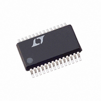
LTC2408CG#PBF Linear Technology, LTC2408CG#PBF Datasheet - Page 24

LTC2408CG#PBF
Manufacturer Part Number
LTC2408CG#PBF
Description
IC A/D CONV 24BIT 8-CHAN 28-SSOP
Manufacturer
Linear Technology
Datasheet
1.LTC2408CGPBF.pdf
(36 pages)
Specifications of LTC2408CG#PBF
Number Of Bits
24
Sampling Rate (per Second)
7.5
Data Interface
MICROWIRE™, Serial, SPI™
Number Of Converters
1
Power Dissipation (max)
1mW
Voltage Supply Source
Single Supply
Operating Temperature
0°C ~ 70°C
Mounting Type
Surface Mount
Package / Case
28-SSOP (0.200", 5.30mm Width)
Number Of Elements
1
Resolution
24Bit
Architecture
Delta-Sigma
Sample Rate
0.008KSPS
Input Polarity
Unipolar
Input Type
Voltage
Rated Input Volt
6.188V
Differential Input
No
Power Supply Requirement
Single
Single Supply Voltage (typ)
3.3/5V
Single Supply Voltage (min)
2.7V
Single Supply Voltage (max)
5.5V
Dual Supply Voltage (typ)
Not RequiredV
Dual Supply Voltage (min)
Not RequiredV
Dual Supply Voltage (max)
Not RequiredV
Differential Linearity Error
1LSB(Typ)
Integral Nonlinearity Error
15ppm of Vref
Operating Temp Range
0C to 70C
Operating Temperature Classification
Commercial
Mounting
Surface Mount
Pin Count
28
Package Type
SSOP
Input Signal Type
Single-Ended
Lead Free Status / RoHS Status
Lead free / RoHS Compliant
Available stocks
Company
Part Number
Manufacturer
Quantity
Price
APPLICATIONS
LTC2404/LTC2408
small valued input capacitors (C
of input source resistance.
For large input capacitor values (C
spikes are averaged by the capacitor into a DC current. The
gain shift becomes a linear function of input source
resistance independent of input capacitance, see Figures
17 and 18. The equivalent input impedance is 1.66M .
This results in 1.5 A of input dynamic current at the
extreme values of V
V
and full-scale readings for every 1
resistance.
While large capacitance applied to one of the multiplexer
channel inputs may result in offset/full-scale shifts, large
24
REF
= 5V). This corresponds to a 0.3ppm shift in offset
Figure 16. Full-Scale Error vs R
–10
–30
–40
–50
–20
50
40
30
20
10
0
Figure 15. Offset vs R
0
1
1
V
V
V
T
A
V
V
V
T
CC
REF
IN
CC
REF
IN
A
= 25 C
= 0V
= 25 C
= 5V
= 5V
= 5V
= 5V
= 5V
10
C
C
C
10
C
IN
C
IN
U
IN
IN
C
IN
C
= 1000pF
IN
IN
C
= 0.01 F
= 1000pF
IN
= 100pF
IN
= 100pF
= 0.01 F
= 0pF
= 0pF
(V
100
R
100
R
SOURCE
INFORMATION
SOURCE
IN
U
= 0V and V
( )
1k
( )
SOURCE
1k
IN
< 0.01 F) as a function
IN
SOURCE
W
10k
10k
> 0.01 F), the input
(Small C)
24048 F15
24048 F16
IN
of input source
100k
(Small C)
100k
= V
REF
U
, when
capacitance applied to the MUXOUT/ADCIN results in
linearity errors. The 75 on-resistance of the multiplexer
switch is nonlinear with input voltage. If the capacitance at
node MUXOUT/ADCIN is less than 0.01 F, the linearity is
not degraded. On the other hand, excessive capacitance
(> 0.01 F) results in incomplete settling as a function of
the multiplexer on-resistance. Hence, the nonlinearity of
the multiplexer switch is seen in the overall transfer
characteristic.
In addition to the input current spikes, the input ESD
protection diodes have a temperature dependent leakage
current. This leakage current, nominally 1nA ( 10nA
max), results in a fixed offset shift of 10 V for a 10k source
resistance.
Figure 18. Full-Scale Error vs R
–100
–150
–200
–250
–300
300
250
200
150
100
–50
50
0
Figure 17. Offset vs R
0
0
0
V
V
V
T
A
CC
REF
IN
100
= 25 C
= 0V
= 5V
= 5V
200
200
C
300
C
IN
IN
= 10 F
= 1 F
400
R
400
R
SOURCE
SOURCE
C
500
IN
C
IN
= 0.01 F
= 0.1 F
600
( )
600
C
( )
C
SOURCE
IN
IN
C
= 10 F
C
700
= 1 F
IN
IN
SOURCE
= 0.1 F
= 0.01 F
800
800
V
V
V
T
(Large C)
A
CC
REF
IN
= 25 C
900
= 5V
24048 F17
= 5V
24048 F18
= 5V
(Large C)
1000
1000


