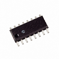
MCP3304-CI/SL Microchip Technology, MCP3304-CI/SL Datasheet - Page 20

MCP3304-CI/SL
Manufacturer Part Number
MCP3304-CI/SL
Description
IC ADC 13BIT 2.7V 4CH SPI 16SOIC
Manufacturer
Microchip Technology
Specifications of MCP3304-CI/SL
Package / Case
16-SOIC (0.154", 3.90mm Width)
Number Of Bits
13
Sampling Rate (per Second)
100k
Data Interface
Serial, SPI™
Number Of Converters
1
Voltage Supply Source
Single Supply
Operating Temperature
-40°C ~ 85°C
Mounting Type
Surface Mount
Architecture
SAR
Conversion Rate
100 KSPs
Resolution
12 bit
Input Type
Voltage
Snr
80.02 dB
Maximum Operating Temperature
+ 85 C
Mounting Style
SMD/SMT
Minimum Operating Temperature
- 40 C
Lead Free Status / RoHS Status
Lead free / RoHS Compliant
Lead Free Status / RoHS Status
Lead free / RoHS Compliant, Lead free / RoHS Compliant
Other names
MCP3304CI/SL
Available stocks
Company
Part Number
Manufacturer
Quantity
Price
Company:
Part Number:
MCP3304-CI/SL
Manufacturer:
MICROCHIP
Quantity:
12 000
Part Number:
MCP3304-CI/SL
Manufacturer:
MICROCHIP/微芯
Quantity:
20 000
MCP3302/04
FIGURE 5-3:
5.2.1
When the MCP3302/04 initiates, charge is stored on
the sample capacitor. When the sample period is
complete, the device converts one bit for each clock
that is received. It is important for the user to note that
a slow clock rate will allow charge to bleed off the
sample cap while the conversion is taking place. For
the MCP330X devices, the recommended minimum
clock speed during the conversion cycle (T
105 kHz. Failure to meet this criteria may induce
linearity errors into the conversion outside the rated
specifications. It should be noted that during the entire
conversion cycle, the
requirements for clock speed or duty cycle, as long as
all timing specifications are met.
5.3
For pseudo-differential bipolar operation, the biasing
circuit (shown in
input AC coupled to the converter. This configuration
will give a digital output range of -4096 to +4095. With
the 2.5V reference, the LSB size equal to 610 µV.
Although the ADC is not production tested with a 2.5V
reference as shown, linearity will not change more than
0.1 LSB. See
INL errors versus V
between the high-pass corner and the acquisition time.
The value of C will need to be quite large in order to
DS21697E-page 20
Legend
I
VA
C
LEAKAGE
SAMPLE
Biasing Solutions
R
C
R
CHx
SS
PIN
SS
R
VA
V
MAINTAINING MINIMUM CLOCK
SPEED
SS
S
T
Figure 2-2
CHx
=
=
=
=
=
=
=
=
=
Figure
signal source
source impedance
input channel pad
input pin capacitance
threshold voltage
leakage current at the pin
due to various junctions
sampling switch
sampling switch resistor
sample/hold capacitance
REF
Analog Input Model.
at V
A/D converter does not have
5-4) shows a single ended
and
DD
7 pF
C
Figure 2-9
PIN
= 5V. A trade-off exists
V
DD
for DNL and
V
V
T
T
= 0.6V
= 0.6V
CONV
) is
I
±1 nA
LEAKAGE
bring down the high-pass corner. The value of R will
need to be 1 kΩ, or less, since higher input
impedances require additional acquisition time. Using
the RC values in
frequency. See
impedance and acquisition time.
FIGURE 5-4:
circuit for bipolar operation.
V
IN
10 µF
C
1 kΩ
1 µF
SS
Sampling
Switch
Figure 2-12
Figure
R
R
S
V
= 1 kΩ
Pseudo-differential biasing
IN+
IN-
OUT
MCP1525
© 2008 Microchip Technology Inc.
5-4, we have a 100 Hz corner
for relation between input
V
MCP330X
SS
C
= DAC capacitance
= 25 pF
V
SAMPLE
IN
0.1 µF
V
REF
V
DD
0.1 µF
= 5V


