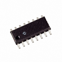
MCP3304-CI/SL Microchip Technology, MCP3304-CI/SL Datasheet - Page 17

MCP3304-CI/SL
Manufacturer Part Number
MCP3304-CI/SL
Description
IC ADC 13BIT 2.7V 4CH SPI 16SOIC
Manufacturer
Microchip Technology
Specifications of MCP3304-CI/SL
Package / Case
16-SOIC (0.154", 3.90mm Width)
Number Of Bits
13
Sampling Rate (per Second)
100k
Data Interface
Serial, SPI™
Number Of Converters
1
Voltage Supply Source
Single Supply
Operating Temperature
-40°C ~ 85°C
Mounting Type
Surface Mount
Architecture
SAR
Conversion Rate
100 KSPs
Resolution
12 bit
Input Type
Voltage
Snr
80.02 dB
Maximum Operating Temperature
+ 85 C
Mounting Style
SMD/SMT
Minimum Operating Temperature
- 40 C
Lead Free Status / RoHS Status
Lead free / RoHS Compliant
Lead Free Status / RoHS Status
Lead free / RoHS Compliant, Lead free / RoHS Compliant
Other names
MCP3304CI/SL
Available stocks
Company
Part Number
Manufacturer
Quantity
Price
Company:
Part Number:
MCP3304-CI/SL
Manufacturer:
MICROCHIP
Quantity:
12 000
Part Number:
MCP3304-CI/SL
Manufacturer:
MICROCHIP/微芯
Quantity:
20 000
4.0
Bipolar Operation - This applies to either a differential
or single ended input configuration, where both positive
and negative codes are output from the A/D converter.
Full bipolar range includes all 8192 codes. For bipolar
operation on a single ended input signal, the A/D
converter must be configured to operate in pseudo
differential mode.
Unipolar Operation - This applies to either a single
ended or differential input signal where only one side of
the device transfer is being used. This could be either
the positive or negative side, depending on which input
(IN+ or IN-) is being used for the DC bias. Full unipolar
operation is equivalent to a 12-bit converter.
Full Differential Operation - Applying a full differential
signal to both the IN(+) and IN(-) inputs is referred to as
full
described in
Pseudo-Differential Operation - Applying a single
ended signal to only one of the input channels with a
bipolar output is referred to as pseudo differential
operation. To obtain a bipolar output from a single
ended input signal the inverting input of the A/D
converter must be biased above V
described in
Integral Nonlinearity - The maximum deviation from a
straight line passing through the endpoints of the
bipolar transfer function is defined as the maximum
integral nonlinearity error. The endpoints of the transfer
function are a point 1/2 LSB above the first code
transition (0x1000) and 1/2 LSB below the last code
transition (0x0FFF).
Differential Nonlinearity - The difference between two
measured adjacent code transitions and the 1 LSB
ideal is defined as differential nonlinearity.
Positive Gain Error - This is the deviation between the
last positive code transition (0x0FFF) and the ideal
voltage level of V
error has been adjusted out.
Negative Gain Error - This is the deviation between
the last negative code transition (0X1000) and the ideal
voltage level of -V
error has been adjusted out.
Offset Error - This is the deviation between the first
positive code transition (0x0001) and the ideal 1/2 LSB
voltage level.
Acquisition Time - The acquisition time is defined as
the time during which the internal sample capacitor is
charging. This occurs for 1.5 clock cycles of the
external CLK as defined in
Conversion Time - The conversion time occurs
immediately after the acquisition time. During this time,
successive approximation of the input signal occurs as
the 13-bit result is being calculated by the internal
circuitry. This occurs for 13 clock cycles of the external
CLK as defined in
© 2008 Microchip Technology Inc.
differential
DEFINITION OF TERMS
Figure
Figure
REF
operation.
REF
Figure
1-5.
1-6.
-1/2 LSB, after the bipolar offset
-1/2 LSB, after the bipolar offset
6-2.
Figure
This
SS
6-2.
. This operation is
configuration
is
Signal-to-Noise Ratio - Signal-to-Noise Ratio (SNR)
is defined as the ratio of the signal-to-noise measured
at the output of the converter. The signal is defined as
the rms amplitude of the fundamental frequency of the
input signal. The noise value is dependant on the
device noise as well as the quantization error of the
converter and is directly affected by the number of bits
in the converter. The theoretical signal-to-noise ratio
limit based on quantization error only for an N-bit
converter is defined as:
EQUATION 4-1:
For a 13-bit converter, the theoretical SNR limit is
80.02 dB.
Total Harmonic Distortion - Total Harmonic Distortion
(THD) is the ratio of the rms sum of the harmonics to
the fundamental, measured at the output of the
converter. For the MCP3302/04, it is defined using the
first 9 harmonics, as is shown in the following equation:
EQUATION 4-2:
Here V
through V
through ninth harmonics.
Signal-to-Noise
combination of SNR and THD. This number represents
the dynamic performance of the converter, including
any harmonic distortion.
EQUATION 4-3:
EffectIve Number of Bits - Effective Number of Bits
(ENOB) states the relative performance of the ADC in
terms of its resolution. This term is directly related to
SINAD by the following equation:
EQUATION 4-4:
For SINAD performance of 78 dB, the effective number
of bits is 12.66. Spurious Free Dynamic Range -
Spurious Free Dynamic Range (SFDR) is the ratio of
the rms value of the fundamental to the next largest
component in ADC’s output spectrum. This is, typically,
the first harmonic, but could also be a noise peak.
Numerically
SINAD(dB)
THD(-dB)
1
is the rms amplitude of the fundamental and V
9
ENOB N
=
are the rms amplitudes of the second
=
SNR
defined,
–
20 log
20 log 10
( )
=
plus
MCP3302/04
----------------------------------------------------------------------------- -
(
=
6.02N
V
SINAD
2
2
SINAD 1.76
----------------------------------
(
+
SNR 10
V
Distortion
+
6.02
2
3
⁄
1.76
+
–
V
)
is
+
2
4
)dB
V
DS21697E-page 17
+
10
2
1
the
.....
–
(
THD 10
+
calculated
(SINAD) -
V
⁄
2
8
+
)
V
2
9
2


