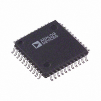
AD73322AST-REEL Analog Devices Inc, AD73322AST-REEL Datasheet - Page 34

AD73322AST-REEL
Manufacturer Part Number
AD73322AST-REEL
Description
IC ANALOG FRONT END DUAL 44-LQFP
Manufacturer
Analog Devices Inc
Datasheet
1.AD73322LARUZ-REEL.pdf
(43 pages)
Specifications of AD73322AST-REEL
Rohs Status
RoHS non-compliant
Number Of Bits
16
Number Of Channels
4
Power (watts)
73mW
Voltage - Supply, Analog
2.7 V ~ 5.5 V
Voltage - Supply, Digital
2.7 V ~ 5.5 V
Package / Case
44-LQFP
AD73322
Grounding and Layout
Since the analog inputs to the AD73322 are differential, most of
the voltages in the analog modulator are common-mode volt-
ages. The excellent common-mode rejection of the part will
remove common-mode noise on these inputs. The analog and
digital supplies of the AD73322 are independent and separately
pinned out to minimize coupling between analog and digital
sections of the device. The digital filters on the encoder section
will provide rejection of broadband noise on the power supplies,
except at integer multiples of the modulator sampling frequency.
The digital filters also remove noise from the analog inputs
provided the noise source does not saturate the analog modula-
tor. However, because the resolution of the AD73322’s ADC is
high, and the noise levels from the AD73322 are so low, care
must be taken with regard to grounding and layout.
The printed circuit board that houses the AD73322 should be
designed so the analog and digital sections are separated and
confined to certain sections of the board. The AD73322 pin
configuration offers a major advantage in that its analog and
digital interfaces are connected on opposite sides of the package.
This facilitates the use of ground planes that can be easily sepa-
rated, as shown in Figure 42. A minimum etch technique is
generally best for ground planes as it gives the best shielding.
Digital and analog ground planes should be joined in only one
place. If this connection is close to the device, it is recommended
to use a ferrite bead inductor as shown in Figure 42.
Avoid running digital lines under the device for they will couple
noise onto the die. The analog ground plane should be allowed
to run under the AD73322 to avoid noise coupling. The power
supply lines to the AD73322 should use as large a trace as pos-
sible to provide low impedance paths and reduce the effects of
glitches on the power supply lines. Fast switching signals such as
clocks should be shielded with digital ground to avoid radiating
noise to other sections of the board, and clock signals should
never be run near the analog inputs. Traces on opposite sides of
the board should run at right angles to each other. This will
reduce the effects of feedthrough through the board. A microstrip
technique is by far the best but is not always possible with a
double-sided board. In this technique, the component side of
the board is dedicated to ground planes while signals are placed
on the other side.
Figure 42. Ground Plane Layout
DIGITAL GROUND
ANALOG GROUND
–34–
Good decoupling is important when using high speed devices.
On the AD73322 both the reference (REFCAP) and supplies
need to be decoupled. It is recommended that the decoupling
capacitors used on both REFCAP and the supplies, be placed as
close as possible to their respective pins to ensure high perfor-
mance from the device. All analog and digital supplies should be
decoupled to AGND and DGND respectively, with 0.1 F
ceramic capacitors in parallel with 10 F tantalum capacitors.
In systems where a common supply voltage is used to drive both
the AVDD and DVDD of the AD73322, it is recommended that
the system’s AVDD supply be used. This supply should have the
recommended analog supply decoupling between the AVDD
pins of the AD73322 and AGND and the recommended digital
supply decoupling capacitors between the DVDD pin and DGND.
DSP PROGRAMMING CONSIDERATIONS
This section discusses some aspects of how the serial port of the
DSP should be configured and the implications of whether Rx
and Tx interrupts should be enabled.
DSP SPORT Configuration
Following are the key settings of the DSP SPORT required for
the successful operation with the AD73322:
• Configure for External SCLK.
• Serial Word Length = 16 bits.
• Transmit and Receive Frame Syncs required with every word.
• Receive Frame Sync is an input to the DSP.
• Transmit Frame Sync is an:
• Frame Syncs occur one SCLK cycle before the MSB of the
• Frame Syncs are active high.
DSP SPORT Interrupts
If SPORT interrupts are enabled, it is important to note that the
active signals on the frame sync pins do not necessarily corre-
spond with the positions in time of where SPORT interrupts are
generated.
On ADSP-21xx processors, it is necessary to enable SPORT
interrupts and use Interrupt Service Routines (ISRs) to handle
Tx/Rx activity, while on the TMS320CSx processors it is pos-
sible to poll the status of the Rx and Tx registers, which means
that Rx/Tx activity can be monitored using a single ISR that
would ideally be the Tx ISR as the Tx interrupt will typically
occur before the Rx ISR.
Input—in Frame Sync Loop-Back Mode
Output—in Nonframe Sync Loop-Back Mode.
serial word.
REV. B


