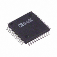
AD73322AST-REEL Analog Devices Inc, AD73322AST-REEL Datasheet - Page 30

AD73322AST-REEL
Manufacturer Part Number
AD73322AST-REEL
Description
IC ANALOG FRONT END DUAL 44-LQFP
Manufacturer
Analog Devices Inc
Datasheet
1.AD73322LARUZ-REEL.pdf
(43 pages)
Specifications of AD73322AST-REEL
Rohs Status
RoHS non-compliant
Number Of Bits
16
Number Of Channels
4
Power (watts)
73mW
Voltage - Supply, Analog
2.7 V ~ 5.5 V
Voltage - Supply, Digital
2.7 V ~ 5.5 V
Package / Case
44-LQFP
AD73322
DESIGN CONSIDERATIONS
The AD73322 features both differential inputs and outputs on
each channel to provide optimal performance and avoid com-
mon mode noise. It is also possible to interface either inputs or
outputs in single-ended mode. This section details the choice of
input and output configurations and also gives some tips to-
wards successful configuration of the analog interface sections.
Analog Inputs
There are several different ways in which the analog input (en-
coder) section of the AD73322 can be interfaced to external
circuitry. It provides optional input amplifiers which allows
sources with high source impedance to drive the ADC section
correctly. When the input amplifiers are enabled, the input
channel is configured as a differential pair of inverting amplifiers
referenced to the internal reference (REFCAP) level. The in-
verting terminals of the input amplifier pair are designated as
pins VINP1 and VINN1 for Channel 1 (VINP2 and VINN2 for
Channel 2) and the amplifier feedback connections are available
on pins VFBP1 and VFBN1 for Channel 1 (VFBP2 and VFBN2
for Channel 2).
For applications where external signal buffering is required,
the input amplifiers can be bypassed and the ADC driven
directly. When the input amplifiers are disabled, the sigma-
delta modulator’s input section (SC PGA) is accessed di-
rectly through the VFBP1 and VFBN1 pins for Channel 1
(VFBP2 and VFBN2 for Channel 2).
It is also possible to drive the ADCs in either differential or
single-ended modes. If the single-ended mode is chosen it is
possible using software control to multiplex between two single-
ended inputs connected to the positive and negative input pins.
The primary concerns in interfacing to the ADC are firstly to
provide adequate anti-alias filtering and to ensure that the signal
source will drive the switched-capacitor input of the ADC
ANTI-ALIAS
0.047 F
0.047 F
FILTER
100
100
Figure 28. Analog Input (DC-Coupled)
VOUTP1
VOUTN1
0.1 F
REFOUT
REFCAP
VFBN1
VFBP1
VINN1
VINP1
V
REF
+6/–15dB
PGA
REFERENCE
GAIN
1
CONTINUOUS
LOW-PASS
FILTER
TIME
AD73322
V
REF
0/38dB
PGA
–30–
correctly. The sigma-delta design of the ADC and its over sam-
pling characteristics simplify the antialias requirements but it
must be remembered that the single pole RC filter is primarily
intended to eliminate aliasing of frequencies above the Nyquist
frequency of the sigma-delta modulator’s sampling rate (typi-
cally 2.048 MHz). It may still require a more specific digital
filter implementation in the DSP to provide the final signal
frequency response characteristics. It is recommended that for
optimum performance that the capacitors used for the antialias-
ing filter be of high quality dielectric (NPO). The second issue
mentioned above is interfacing the signal source to the ADC’s
switched capacitor input load. The SC input presents a complex
dynamic load to a signal source, therefore, it is important to
understand that the slew rate characteristic is an important
consideration when choosing external buffers for use with the
AD73322. The internal inverting op amps on the AD73322 are
specifically designed to interface to the ADC’s SC input stage.
The AD73322’s on-chip 38 dB preamplifier can be enabled
when there is not enough gain in the input circuit; the preampli-
fier is configured by bits IGS0-2 of CRD. The total gain must
be configured to ensure that a full-scale input signal produces a
signal level at the input to the sigma-delta modulator of the
ADC that does not exceed the maximum input range.
The dc biasing of the analog input signal is accomplished with
an on-chip voltage reference. If the input signal is not biased at
the internal reference level (via REFOUT), then it must be
ac-coupled with external coupling capacitors. C
0.1 F or larger. The dc biasing of the input can then be accom-
plished using resistors to REFOUT as in Figures 31 and 32.
Figure 29. Analog Input (DC-Coupled) Using External
Amplifiers
OPTIONAL
BUFFER
ANTI-ALIAS
FILTER
100
0.047
0.047
100
F
F
VOUTP1
0.1 F
VOUTN1
REFOUT
REFCAP
VFBN1
VFBP1
VINN1
VINP1
V
REF
+6/–15dB
PGA
REFERENCE
GAIN
1
CONTINUOUS
LOW-PASS
FILTER
TIME
IN
should be
AD73322
V
REF
REV. B
0/38dB
PGA


