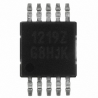
ISL1219IUZ Intersil, ISL1219IUZ Datasheet - Page 17

ISL1219IUZ
Manufacturer Part Number
ISL1219IUZ
Description
IC RTC LP BATT BACK SRAM 10MSOP
Manufacturer
Intersil
Type
Clock/Calendar/NVSRAMr
Specifications of ISL1219IUZ
Memory Size
2B
Time Format
HH:MM:SS (12/24 hr)
Date Format
YY-MM-DD-dd
Interface
I²C, 2-Wire Serial
Voltage - Supply
2.7 V ~ 5.5 V
Operating Temperature
-40°C ~ 85°C
Mounting Type
Surface Mount
Package / Case
10-MSOP, Micro10™, 10-uMAX, 10-uSOP
Clock Format
HH
Clock Ic Type
RTC
Interface Type
I2C, Serial
Memory Configuration
2 X 8
Supply Voltage Range
2.7V To 5.5V
Digital Ic Case Style
MSOP
Rohs Compliant
Yes
Lead Free Status / RoHS Status
Lead free / RoHS Compliant
Available stocks
Company
Part Number
Manufacturer
Quantity
Price
Company:
Part Number:
ISL1219IUZ
Manufacturer:
Intersil
Quantity:
490
Company:
Part Number:
ISL1219IUZ
Manufacturer:
Intersil
Quantity:
222
Part Number:
ISL1219IUZ-T
Manufacturer:
INTERSIL
Quantity:
20 000
Note: xx indicate other control bits
After these registers are set, an alarm will be generated when
the RTC advances to exactly 11:30am on January 1 (after
seconds changes from 59 to 00) by setting the ALM bit in the
status register to “1” and also bringing the IRQ output low.
Example 2 – Pulsed interrupt once per minute (IM = “1”)
Interrupts at one minute intervals when the seconds register
is at 30 seconds.
A. Set Alarm registers as follows:
B. Set the Interrupt register as follows:
Note: xx indicate other control bits
Once the registers are set, the following waveform will be
seen at IRQ-:
Note that the status register ALM bit will be set each time the
alarm is triggered, but does not need to be read or cleared.
User Registers
Addresses [12h to 13h]
These registers are 2 bytes of battery-backed user memory
storage.
Time Stamp Registers
Addresses [14h to 19h]
These registers contain the time stamp information in a similar
format to the RTC registers. When a valid Event is triggered at
the EVIN pin (low to high transition), these registers record the
REGISTER
REGISTER
CONTROL
ALARM
DWA
MNA
MOA
SCA
HRA
DTA
INT
RTC AND ALARM REGISTERS ARE BOTH “30” SEC
7 6 5 4 3 2 1 0 HEX
1 1 x x 0 0 0 0 x0h Enable Alarm and Int
7 6 5 4 3 2 1 0 HEX
1 0 1 1 0 0 0 0 B0h Seconds set to 30,
0 0 0 0 0 0 0 0 00h Minutes disabled
0 0 0 0 0 0 0 0 00h Hours disabled
0 0 0 0 0 0 0 0 00h Date disabled
0 0 0 0 0 0 0 0 00h Month disabled
0 0 0 0 0 0 0 0 00h Day of week disabled
BIT
BIT
60 SEC
17
Mode
enabled
DESCRIPTION
DESCRIPTION
ISL1219
values from the RTC registers. At the same time the EVT bit is
set and the EVDET- pin changes state (if it is enabled). The six
registers include second, minute, hour, date, month and year of
the event. Day of week is not recorded as it is not normally
required and is arbitrarily set.
Only the first Event in a series of events is time stamped, all
subsequent events are ignored. The current time stamp is
retained until the EVT bit is cleared and the next Event
occurs (EVIN pin is triggered). The contents of these
registers are cleared only after full power cycling.
I
The ISL1219 supports a bidirectional bus oriented protocol.
The protocol defines any device that sends data onto the
bus as a transmitter and the receiving device as the receiver.
The device controlling the transfer is the master and the
device being controlled is the slave. The master always
initiates data transfers and provides the clock for both
transmit and receive operations. Therefore, the ISL1219
operates as a slave device in all applications.
All communication over the I
sending the MSB of each byte of data first.
Protocol Conventions
Data states on the SDA line can change only during SCL
LOW periods. SDA state changes during SCL HIGH are
reserved for indicating START and STOP conditions.
the input mode.
All I
condition, which is a HIGH to LOW transition of SDA while
SCL is HIGH. The ISL1219 continuously monitors the SDA
and SCL lines for the START condition and does not
respond to any command until this condition is met.
power-up sequence.
All I
condition, which is a LOW to HIGH transition of SDA while
SCL is HIGH (Figure 14). A STOP condition at the end of a
read operation or at the end of a write operation to memory
only places the device in its standby mode.
An acknowledge (ACK) is a software convention used to
indicate a successful data transfer. The transmitting device,
either master or slave, releases the SDA bus after
transmitting eight bits. During the ninth clock cycle, the
receiver pulls the SDA line LOW to acknowledge the
reception of the eight bits of data (Figure 15).
The ISL1219 responds with an ACK after recognition of a
START condition followed by a valid Identification Byte, and
once again after successful receipt of an Address Byte. The
ISL1219 also responds with an ACK after receiving a Data
Byte of a write operation. The master must respond with an
ACK after receiving a Data Byte of a read operation.
(Figure 14). On power up of the ISL1219, the SDA pin is in
2
(Figure 14). A START condition is ignored during the
C Serial Interface
2
2
C interface operations must begin with a START
C interface operations must be terminated by a STOP
2
C interface is conducted by
July 15, 2010
FN6314.2


