ISL1219IUZ Intersil, ISL1219IUZ Datasheet - Page 14
ISL1219IUZ
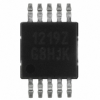
Manufacturer Part Number
ISL1219IUZ
Description
IC RTC LP BATT BACK SRAM 10MSOP
Manufacturer
Intersil
Type
Clock/Calendar/NVSRAMr
Specifications of ISL1219IUZ
Memory Size
2B
Time Format
HH:MM:SS (12/24 hr)
Date Format
YY-MM-DD-dd
Interface
I²C, 2-Wire Serial
Voltage - Supply
2.7 V ~ 5.5 V
Operating Temperature
-40°C ~ 85°C
Mounting Type
Surface Mount
Package / Case
10-MSOP, Micro10™, 10-uMAX, 10-uSOP
Clock Format
HH
Clock Ic Type
RTC
Interface Type
I2C, Serial
Memory Configuration
2 X 8
Supply Voltage Range
2.7V To 5.5V
Digital Ic Case Style
MSOP
Rohs Compliant
Yes
Lead Free Status / RoHS Status
Lead free / RoHS Compliant
Available stocks
Company
Part Number
Manufacturer
Quantity
Price
Company:

Part Number:
ISL1219IUZ
Manufacturer:
Intersil
Quantity:
490
Company:
Part Number:
ISL1219IUZ
Manufacturer:
Intersil
Quantity:
222
Part Number:
ISL1219IUZ-T
Manufacturer:
INTERSIL
Quantity:
20 000


AUTO RESET ENABLE BIT (ARST)
This bit enables/disables the automatic reset of the BAT and
ALM, EVT status bits only. When ARST bit is set to “1”, these
status bits are reset to “0” after a valid read of the Status
Register (with a valid STOP condition). When the ARST is
cleared to “0”, the user must manually reset the BAT, ALM,
and EVT bits.
INTERRUPT CONTROL REGISTER (INT)
The interrupt control register contains Frequency Output,
Alarm, and Battery switchover control bits.
NOTE: Writing to register 08h has restrictions. If V
byte writes to register 08h are allowed, only page writes beginning
with register 07h. If V
allowed, as well as page writes.
FREQUENCY OUT CONTROL BITS (FO <3:0>)
These bits enable/disable the frequency output function and
select the output frequency at the IRQ/F
Table 8 for frequency selection. When the frequency mode is
enabled, it will override the alarm mode at the IRQ/F
FREQUENCY OUTPUT AND INTERRUPT BIT (FOBATB)
This bit enables/disables the F
backup mode (i.e. V
08h
Default
ADDR
FREQUENCY,
32768
F
TABLE 8. FREQUENCY SELECTION OF F
4096
1024
TABLE 7. INTERRUPT CONTROL REGISTER (INT)
1/16
1/32
OUT
1/2
1/4
1/8
64
32
16
0
8
4
2
1
IM ALME LPMODE FOBATB FO3 FO2 FO1 FO0
7
0
6
0
UNITS
DD
Hz
Hz
Hz
Hz
Hz
Hz
Hz
Hz
Hz
Hz
Hz
Hz
Hz
Hz
Hz
Hz
BAT
>V
5
0
BAT
power source active). When the
FO3
, then a byte write to register 08h IS
0
0
0
0
0
0
0
0
1
1
1
1
1
1
1
1
14
OUT
4
0
/IRQ pin during battery
FO2
0
0
0
0
1
1
1
1
0
0
0
0
1
1
1
1
OUT
3
0
BAT
pin. See
FO1
OUT
0
0
1
1
0
0
1
1
0
0
1
1
0
0
1
1
2
0
>V
DD
PIN
1
0
OUT
, then no
FO0
0
1
0
1
0
1
0
1
0
1
0
1
0
1
0
1
pin.
0
0
ISL1219
FOBATB is set to “1” the F
battery backup mode. This means that both the frequency
output and alarm output functions are disabled. When the
FOBATB is cleared to “0”, the F
during battery backup mode.
LOW POWER MODE BIT (LPMODE)
This bit enables/disables low power mode. With
LPMODE = “0”, the device will be in normal mode and the
V
V
power mode and the V
V
about 600nA when using LPMODE = “1” with V
Typical Performance Curves: I
& OFF on page 6).
It should be noted that any writes to the LPMODE bit that
may put the device into Low Power Mode should be avoided
if V
the I
ALARM ENABLE BIT (ALME)
This bit enables/disables the alarm function. When the ALME
bit is set to “1”, the alarm function is enabled. When the ALME
is cleared to “0”, the alarm function is disabled. The alarm
function can operate in either a single event alarm or a periodic
interrupt alarm (see IM bit).
NOTE: When the frequency output mode is enabled, the alarm function
is disabled.
INTERRUPT/ALARM MODE BIT (IM)
This bit enables/disables the interrupt mode of the alarm
function. When the IM bit is set to “1”, the alarm will operate
in the interrupt mode, where an active low pulse width of
250ms will appear at the IRQ/F
triggered by the alarm as defined by the alarm registers (0Ch
to 11h). When the IM bit is cleared to “0”, the alarm will
operate in standard mode, where the IRQ/F
tied low until the ALM status bit is cleared to “0”.
EVENT DETECTION REGISTER (EV)
The ISL1219 provides an easy to use event and tamper
detection circuit. The Event Detection Register configures
the functionality of the event detection circuits.
EVENT INPUT SAMPLING SELECTION BITS
(ESMP<1:0>)
These two bits select the rate of sampling of the EVIN pin to
trigger an event detection. For example, a 2Hz sampling rate
would configure the ISL1219 to check the status of the EV
BAT
DD
DD
DD
2
< V
< V
C interface (until V
supply will be used when V
IM BIT
<V
TRIP
0
1
BAT
BAT
, as the device will no longer communicate over
. With LPMODE = “1”, the device will be in low
- V
BATHYS
Single Time Event Set By Alarm
Repetitive/Recurring Time Event Set By Alarm
BAT
INTERRUPT/ALARM FREQUENCY
DD
. There is a supply current saving of
TABLE 9.
OUT
supply will be used when
rises above V
DD
/IRQ pin is disabled during
OUT
OUT
DD
vs V
/IRQ pin is enabled
pin when the RTC is
< V
DD
BAT
BAT
with LPMODE ON
OUT
- V
).
DD
BATHYS
pin will be
= 5V. (see
July 15, 2010
FN6314.2
and
Related parts for ISL1219IUZ
Image
Part Number
Description
Manufacturer
Datasheet
Request
R

Part Number:
Description:
Real Time Clock/Calendar
Manufacturer:
Intersil Corporation
Datasheet:
Part Number:
Description:
Intersil Corporation [CMOS Serial Controller Interface]
Manufacturer:
Intersil Corporation
Datasheet:
Part Number:
Description:
Manufacturer:
Intersil Corporation
Datasheet:
Part Number:
Description:
357-036-542-201 CARDEDGE 36POS DL .156 BLK LOPRO
Manufacturer:
Intersil Corporation
Datasheet:
Part Number:
Description:
1024-Word x 4-Bit LSI Static RAM
Manufacturer:
Intersil Corporation
Datasheet:
Part Number:
Description:
General Purpose NPN Transistor Arrays FN341.4
Manufacturer:
Intersil Corporation
Datasheet:
Part Number:
Description:
CMOS 16-Bit Microprocessor
Manufacturer:
Intersil Corporation
Datasheet:
Part Number:
Description:
Manufacturer:
Intersil Corporation
Datasheet:
Part Number:
Description:
Manufacturer:
Intersil Corporation
Datasheet:
Part Number:
Description:
Manufacturer:
Intersil Corporation
Datasheet:
Part Number:
Description:
Manufacturer:
Intersil Corporation
Datasheet:
Part Number:
Description:
CMOS 6-Bit Latch and Decoder Memory Interfaces
Manufacturer:
Intersil Corporation
Datasheet:
Part Number:
Description:
CA3046General Purpose NPN Transistor Arrays
Manufacturer:
Intersil Corporation
Datasheet:
Part Number:
Description:
Manufacturer:
Intersil Corporation
Datasheet:
Part Number:
Description:
TR909 DLC/FLC SLIC with Low Power Standby
Manufacturer:
Intersil Corporation
Datasheet: