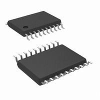
LMX2433TMX/NOPB National Semiconductor, LMX2433TMX/NOPB Datasheet - Page 29

LMX2433TMX/NOPB
Manufacturer Part Number
LMX2433TMX/NOPB
Description
IC SYNTHESIZER DL 3.6GHZ 20TSSOP
Manufacturer
National Semiconductor
Series
PLLatinum™r
Type
PLL Frequency Synthesizerr
Datasheet
1.LMX2433SLEXNOPB.pdf
(49 pages)
Specifications of LMX2433TMX/NOPB
Pll
Yes with Bypass
Input
CMOS
Output
CMOS
Number Of Circuits
1
Ratio - Input:output
3:2
Differential - Input:output
Yes/No
Frequency - Max
3.6GHz, 1.7GHz
Divider/multiplier
No/No
Voltage - Supply
2.25 V ~ 2.75 V
Operating Temperature
-40°C ~ 85°C
Mounting Type
Surface Mount
Package / Case
20-TSSOP
Frequency-max
3.6GHz
For Use With
LMX2433EVAL - EVALUATION BOARD FOR LMX2433
Lead Free Status / RoHS Status
Lead free / RoHS Compliant
Other names
LMX2433TMX
LMX243x Charge Pump Test Setup
The block diagram above illustrates the setup required to
measure the LMX243x device’s RF charge pump sink cur-
rent. The same setup is used for the LMX2430TM Evaluation
Board. The purpose of this test is to assess the functionality
of the RF charge pump. The IF charge pump is evaluated in
the same way.
This setup uses an open loop configuration. A power supply
is connected to Vcc. By means of a signal generator, a 10
MHz signal is typically applied to the FinRF pin. The signal is
one of two inputs to the phase/ frequency detector (PFD).
The 3 dB pad provides a 50Ω match between the PLL and
the signal generator. The OSCin pin is tied to Vcc. This
establishes the other input to the PFD. Alternatively, this
input can be tied directly to the ground plane. The EN and
ENosc pins are also both tied to Vcc. A Semiconductor
Parameter Analyzer is connected to the CPoutRF pin and
used to measure the sink, source, and TRI-STATE leakage
currents.
Let F
OSCin pin, which is simply zero in this case (DC), and let F
represent the frequency of the signal applied to the FinRF
r
represent the frequency of the signal applied to the
p
29
pin. The PFD is sensitive to the rising edges of F
Assuming positive VCO characteristics (RF_CPP bit = 1);
the charge pump turns ON, and sinks current when the first
rising edge of F
charge pump continues to sink current indefinitely. In order
to measure the RF charge pump source current, the
RF_CPP bit is simply set to 0 (negative VCO characteristics)
in CodeLoader. Similarly, in order to measure the TRI-STATE
leakage current, the RF_CPT bit is set to 1.
The measurements are typically taken over supply voltage
and temperature. The measurements are also typically taken
at the HIGH and LOW charge pump current gains. The
charge pump current gain can be controlled by the RF_CPG
bit in CodeLoader. Once the charge pump currents are
determined, the (i) charge pump output current magnitude
variation versus charge pump output voltage, (ii) charge
pump output sink current versus charge pump output source
current mismatch, and (iii) charge pump output current mag-
nitude versus tempeature, can be calculated. Refer to the
Charge Pump Current Specifications Definition for more
details.
p
is detected. Since F
r
has no rising edge, the
www.national.com
20053588
r
and F
p
.


