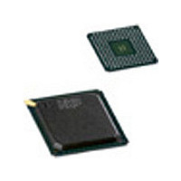
PNX1311EH/G NXP Semiconductors, PNX1311EH/G Datasheet - Page 521

PNX1311EH/G
Manufacturer Part Number
PNX1311EH/G
Description
Manufacturer
NXP Semiconductors
Datasheet
1.PNX1311EHG.pdf
(548 pages)
Specifications of PNX1311EH/G
Lead Free Status / RoHS Status
Compliant
- Current page: 521 of 548
- Download datasheet (6Mb)
Philips Semiconductors
Figure C-6. Packed YUV 4:2:2+α data format for the ICP or VO in Little and Big Endian modes
Figure C-7. Packed YUV 4:2:2 data format for ICP in Little and Big Endian modes
Figure C-8. RBG-16 data format for ICP in Little and Big Endian modes
Pixel half-word data
in memory or PCI
Pixel half-word data
in memory or PCI
Pixel half-word data
in memory or PCI
31
31
31
V1α3
A+3
V0α1
A+3
G1B1
G3B3
V0
V1
A+3
P
P
P
n+1
n+1
n+1
Big Endian Mode
Big Endian Mode
A+2
A+2
Big Endian Mode
Y3
R1G’1
Y1
Y1
R3G’3
Y3
A+2
A+1
A+1
U1α2
U0α0
U1
G0B0
G2B2
U0
A+1
Note: A+0 corresponds to byte-0 lane of SDRAM/Hwy/PCI
Note: A+0 corresponds to byte-0 lane of SDRAM/Hwy/PCI
Note: A+0 corresponds to byte-0 lane of SDRAM/Hwy/PCI
and A+3 corresponds to byte-3 lane of SDRAM/Hwy/PCI
and A+3 corresponds to byte-3 lane of SDRAM/Hwy/PCI
and A+3 corresponds to byte-3 lane of SDRAM/Hwy/PCI
P
P
P
n
n
n
PRELIMINARY SPECIFICATION
A+0
A+0
Y0
Y2
Y0
Y2
R2G’2
A+0
R0G’0
0
0
0
31
31
31
R3G’3
R1G’1
A+3
A+3
Y1
Y3
Y1
Y3
A+3
P
P
P
n+1
n+1
Little Endian Mode
Little Endian Mode
Little Endian Mode
n+1
V0α1
V1α3
A+2
A+2
V0
V1
G1B1
G3B3
A+2
A+1
A+1
R2G’2
R0G’0
A+1
Y0
Y2
Y0
Y2
Endian-ness
P
P
P
n
n
n
U0α0
U1α2
A+0
A+0
U0
U1
G0B0
G2B2
A+0
0
0
C-5
0
Related parts for PNX1311EH/G
Image
Part Number
Description
Manufacturer
Datasheet
Request
R
Part Number:
Description:
NXP Semiconductors designed the LPC2420/2460 microcontroller around a 16-bit/32-bitARM7TDMI-S CPU core with real-time debug interfaces that include both JTAG andembedded trace
Manufacturer:
NXP Semiconductors
Datasheet:

Part Number:
Description:
NXP Semiconductors designed the LPC2458 microcontroller around a 16-bit/32-bitARM7TDMI-S CPU core with real-time debug interfaces that include both JTAG andembedded trace
Manufacturer:
NXP Semiconductors
Datasheet:
Part Number:
Description:
NXP Semiconductors designed the LPC2468 microcontroller around a 16-bit/32-bitARM7TDMI-S CPU core with real-time debug interfaces that include both JTAG andembedded trace
Manufacturer:
NXP Semiconductors
Datasheet:
Part Number:
Description:
NXP Semiconductors designed the LPC2470 microcontroller, powered by theARM7TDMI-S core, to be a highly integrated microcontroller for a wide range ofapplications that require advanced communications and high quality graphic displays
Manufacturer:
NXP Semiconductors
Datasheet:
Part Number:
Description:
NXP Semiconductors designed the LPC2478 microcontroller, powered by theARM7TDMI-S core, to be a highly integrated microcontroller for a wide range ofapplications that require advanced communications and high quality graphic displays
Manufacturer:
NXP Semiconductors
Datasheet:
Part Number:
Description:
The Philips Semiconductors XA (eXtended Architecture) family of 16-bit single-chip microcontrollers is powerful enough to easily handle the requirements of high performance embedded applications, yet inexpensive enough to compete in the market for hi
Manufacturer:
NXP Semiconductors
Datasheet:
Part Number:
Description:
The XA-S3 device is a member of Philips Semiconductors? XA(eXtended Architecture) family of high performance 16-bitsingle-chip microcontrollers
Manufacturer:
NXP Semiconductors
Datasheet:

Part Number:
Description:
The NXP BlueStreak LH75401/LH75411 family consists of two low-cost 16/32-bit System-on-Chip (SoC) devices
Manufacturer:
NXP Semiconductors
Datasheet:

Part Number:
Description:
The NXP LPC3130/3131 combine an 180 MHz ARM926EJ-S CPU core, high-speed USB2
Manufacturer:
NXP Semiconductors
Datasheet:

Part Number:
Description:
The NXP LPC3141 combine a 270 MHz ARM926EJ-S CPU core, High-speed USB 2
Manufacturer:
NXP Semiconductors

Part Number:
Description:
The NXP LPC3143 combine a 270 MHz ARM926EJ-S CPU core, High-speed USB 2
Manufacturer:
NXP Semiconductors

Part Number:
Description:
The NXP LPC3152 combines an 180 MHz ARM926EJ-S CPU core, High-speed USB 2
Manufacturer:
NXP Semiconductors

Part Number:
Description:
The NXP LPC3154 combines an 180 MHz ARM926EJ-S CPU core, High-speed USB 2
Manufacturer:
NXP Semiconductors

Part Number:
Description:
Standard level N-channel enhancement mode Field-Effect Transistor (FET) in a plastic package using NXP High-Performance Automotive (HPA) TrenchMOS technology
Manufacturer:
NXP Semiconductors
Datasheet:


