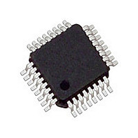
MC34911G5ACR2 Freescale, MC34911G5ACR2 Datasheet - Page 79

MC34911G5ACR2
Manufacturer Part Number
MC34911G5ACR2
Description
Manufacturer
Freescale
Datasheet
1.MC34911G5ACR2.pdf
(92 pages)
Specifications of MC34911G5ACR2
Turn Off Delay Time
10us
Number Of Drivers
2
Operating Temperature (min)
-40C
Lead Free Status / RoHS Status
Compliant
Available stocks
Company
Part Number
Manufacturer
Quantity
Price
Company:
Part Number:
MC34911G5ACR2
Manufacturer:
Freescale Semiconductor
Quantity:
10 000
33911 SPI INTERFACE AND CONFIGURATION
link between a microcontroller (master) and the 33911.
transfer is prepared.
transfer and puts the MISO in the low-impedance state and
latches the analog status data (Register read data).
moved to MISO/MOSI pins. With the falling edge of the SPI
clock (SCLK), the data is sampled by the receiver.
edges are present during the active (low) phase of
79
33911
FUNCTIONAL DEVICE OPERATIONS
LOGIC COMMANDS AND REGISTERS
The serial peripheral interface creates the communication
The interface consists of four pins (see
•
• MOSI — Master-Out Slave-In
During the inactive phase of the
The falling edge of the
With the rising edge of the SPI clock (SCLK), the data is
The data transfer is only valid if exactly 8 sample clock
CS
— Chip Select
SCLK
MOSI
MISO
Change MISO/MISO Output
CS
Read Data Latch
Rising Edge of SCLK
CS
indicates the start of a new data
CS
(HIGH), the new data
LOGIC COMMANDS AND REGISTERS
Figure
VMS LINS HSS
A3
Falling Edge of SCLK
Sample MISO/MISO Input
43):
A2
CS
Figure 43. SPI Protocol
.
A1
Register Read Data
Register Write Data
A0
LSS
The master sends 4 bits of address (A3:A0) + 4 bits of control
information (C3:C0) and the slave replies with 4 system
status bits (VMS,LINS,HSS,LSS) + 4 bits of status
information (S3:S0).
of the transfer and latches the write data (MOSI) into the
register. The
state.
condition. Reset condition is the condition causing the bit to
be set to its reset value. The main reset conditions are:
and BATFAIL flag sets.
C3
S3
• MISO — Master-In Slave-Out
• SCLK— Serial Clock
A complete data transfer via the SPI consists of 1 byte.
The rising edge of the Chip Select (
Register reset values are described along with the reset
- Power-On Reset (POR): level at which the logic is reset
- Reset mode
- Reset done by the RST pin (ext_reset)
C2
S2
CS
C1
S1
high forces MISO to the high-impedance
C0
S0
Analog Integrated Circuit Device Data
Write Data Latch
Freescale Semiconductor
CS)
indicates the end


