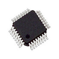
MC34911G5ACR2 Freescale, MC34911G5ACR2 Datasheet - Page 27

MC34911G5ACR2
Manufacturer Part Number
MC34911G5ACR2
Description
Manufacturer
Freescale
Datasheet
1.MC34911G5ACR2.pdf
(92 pages)
Specifications of MC34911G5ACR2
Turn Off Delay Time
10us
Number Of Drivers
2
Operating Temperature (min)
-40C
Lead Free Status / RoHS Status
Compliant
Available stocks
Company
Part Number
Manufacturer
Quantity
Price
Company:
Part Number:
MC34911G5ACR2
Manufacturer:
Freescale Semiconductor
Quantity:
10 000
INTRODUCTION
(Run), Stop, and Sleep (Low Power). In Normal mode, the
device is active and is operating under normal application
conditions. The Stop and Sleep modes are low power modes
with wake-up capabilities.
with V
voltage regulator is turned off (V
interrupt. Wake-up from Sleep mode is done by a reset and
the voltage regulator is turned back on.
MOD1:2 bits in the Mode Control Register (MCR).
different operating modes.
operating modes.
RESET MODE
mode, the RST pin is low for 1.0 ms (typical value). After this
delay, it enters the Normal Request mode and the RST pin is
driven high.
low, watchdog trigger fail, after wake-up from Sleep mode,
Normal Request mode timeout occurs).
NORMAL REQUEST MODE
device after the Reset mode, or after a wake-up from Stop
mode.
RESET pin is High, and the LIN is operating in RX Only
mode.
an internal timer is started for 150 ms (typical value). During
these 150 ms, the MCU must configure the Timing Control
Register (TIMCR) and the Mode Control Register (MCR) with
MOD2 and MOD1 bits set = 0, to enter the Normal mode. If
within the 150 ms timeout, the MCU does not command the
33911 to Normal mode, it will enter in Reset mode. If the
WDCONF pin is grounded in order to disable the watchdog
function, it goes directly in Normal mode after the Reset
mode.
NORMAL MODE
controlled by the SPI interface and the PWMIN pin.
Analog Integrated Circuit Device Data
Freescale Semiconductor
The 33911 offers three main operating modes: Normal
In Stop mode, the voltage regulator still supplies the MCU
Wake-up from Stop mode is initiated by a wake-up
The selection of the different modes is controlled by the
Figure 14
The 33911 enters the Reset mode after a power up. In this
The Reset mode is entered if a reset condition occurs (V
This is a temporary mode automatically accessed by the
In Normal Request mode, the VDD regulator is ON, the
As soon as the device enters in the Normal Request mode
In Normal mode, all 33911 functions are active and can be
DD
(limited current capability), while in Sleep mode the
describes how transitions are done between the
Table
DD
6, gives an overview of the
= 0 V).
FUNCTIONAL DEVICE OPERATIONS
OPERATIONAL MODES
DD
capability.
pin and the Ground, the window watchdog function will be
enabled.
inputs or have its voltage routed through the analog-
multiplexer.
the LIN protocol specification 2.0, 2.1 and SAEJ2602. The
LIN bus can transmit and receive information.
PWM capability according to the SPI configuration.
over/under-voltage, thermal shutdown, or thermal shutdown
prewarning on the main regulator.
SLEEP MODE
mode, the device enters into Sleep mode by sending one SPI
command through the Mode Control Register (MCR), or (V
low > 150 ms) with V
under-voltage condition with no V
0) will send the device to Sleep mode. All blocks are in their
lowest power consumption condition. Only some wake-up
sources (wake-up inputs with or without cyclic sense, forced
wake-up and LIN receiver) are active. The 5.0 V regulator is
OFF. The internal low-power oscillator may be active if the IC
is configured for cyclic-sense. In this condition, the high side
switch is turned on periodically and the wake-up inputs are
sampled.
device goes in Reset mode except that the SPI will report the
wake-up source and the BATFAIL flag is not set.
STOP MODE
case the 5.0 V regulator is ON with limited current drive
capability. The application MCU is always supplied while the
33911 is operating in Stop mode.
SPI command. When the application is in this mode, it can
wake-up from the 33911 side (for example: cyclic sense,
force wake-up, LIN bus, wake inputs) or the MCU side (CS,
RST pins). Wake-up from Stop mode will transition the 33911
to Normal Request mode and generates an interrupt except
if the wake-up event is a low to high transition on the CS pin
or comes from the RST pin.
The VDD regulator is ON and delivers its full current
If an external resistor is connected between the WDCONF
The wake-up inputs (L1 and L2) can be read as digital
The LIN interface has slew rate and timing compatible with
The high side and low side switches are active and have
The interrupts are generated to report failures for V
The Sleep mode is a low power mode. From Normal
Wake-up from Sleep mode is similar to a power-up. The
The Stop mode is the second low power mode, but in this
The device can enter into Stop mode only by sending the
SUV
FUNCTIONAL DEVICE OPERATIONS
= 0. When in Reset mode, a V
SUP
OPERATIONAL MODES
under-voltage (V
SUP
SUV
33911
DD
DD
27
=


