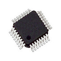
MC34911G5ACR2 Freescale, MC34911G5ACR2 Datasheet - Page 6

MC34911G5ACR2
Manufacturer Part Number
MC34911G5ACR2
Description
Manufacturer
Freescale
Datasheet
1.MC34911G5ACR2.pdf
(92 pages)
Specifications of MC34911G5ACR2
Turn Off Delay Time
10us
Number Of Drivers
2
Operating Temperature (min)
-40C
Lead Free Status / RoHS Status
Compliant
Available stocks
Company
Part Number
Manufacturer
Quantity
Price
Company:
Part Number:
MC34911G5ACR2
Manufacturer:
Freescale Semiconductor
Quantity:
10 000
Table 2. 33911 Pin Definitions
6
33911
Notes
PIN CONNECTIONS
15,16, 20 &
1.
2.
3.
4.
A functional description of each pin can be found in the
Pin
12
13
14
21
17
19
18
22
23
24
25
26
27
28
29
31
32
When used as digital input, a series 33 kΩ resistor must be used to protect against automotive transients.
Reverse battery protection series diodes must be used externally to protect the internal circuitry.
This pin can be connected directly to the battery line for voltage measurements. The pin is self protected against reverse battery
connections. It is strongly recommended to connect a 10 kΩ resistor in series with this pin for protection purposes.
External capacitor (2.0 µF < C < 100 µF; 0.1 Ω < ESR < 10 Ω) required.
Pin Name
WDCONF
VSENSE
PGND
AGND
LGND
VDD
HS1
LS2
LS1
VS2
VS1
LIN
NC
NC
NC
L2
L1
Analog Ground Pin
Power Ground Pin
Voltage Sense Pin
Voltage Regulator
Low Side Outputs
Power Supply Pin
Configuration Pin
High Side Output
LIN Ground Pin
Wake-up Inputs
Not Connected
Not Connected
Not Connected
Formal Name
Watchdog
LIN Bus
Output
This input pin is for configuration of the watchdog period and allows the
disabling of the watchdog.
This pin represents the single-wire bus transmitter and receiver.
This pin is the device LIN ground connection. It is internally connected to the
PGND pin.
This pin must not be connected or connected to ground.
Relay drivers low side outputs.
This pin is the device low side ground connection. It is internally connected to
the LGND pin.
These pins are the wake-up capable digital inputs
can be sensed analog via the analog multiplexer.
This pin must not be connected or connected to VS2.
High side switch output.
These pins are device battery level power supply pins. VS2 is supplying the
HS1 driver while VS1 supplies the remaining blocks.
This pin can be left opening or connected to any potential ground or power
supply
Battery voltage sense input.
+5.0 V main voltage regulator output pin.
This pin is the device analog ground connection.
Functional Pin Description
(3)
section beginning on
Definition
Analog Integrated Circuit Device Data
(4)
Freescale Semiconductor
(1)
. In addition, all Lx inputs
(2)
page
24.


