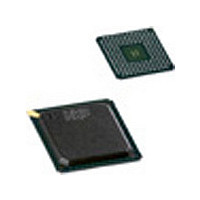
SAA7118EEB-T NXP Semiconductors, SAA7118EEB-T Datasheet - Page 18

SAA7118EEB-T
Manufacturer Part Number
SAA7118EEB-T
Description
Video ICs COMPONENT VID DECODER W/COMB F
Manufacturer
NXP Semiconductors
Type
Multi-Standard Video Decoderr
Datasheet
1.SAA7118EEB-T.pdf
(177 pages)
Specifications of SAA7118EEB-T
Adc/dac Resolution
9b
Screening Level
Commercial
Package Type
LBGA
Pin Count
156
Maximum Operating Temperature
+ 70 C
Package / Case
SOT-700
Minimum Operating Temperature
0 C
Mounting Style
SMD/SMT
Lead Free Status / RoHS Status
Not Compliant
Other names
SAA7118E/V1,518
- Current page: 18 of 177
- Download datasheet (906Kb)
NXP Semiconductors
SAA7118_7
Product data sheet
8.1.1.2 Gain control
The gain control circuit receives (via the I
amplifiers or controls one of these amplifiers automatically via a built-in Automatic Gain
Control (AGC) as part of the Analog Input COntrol (AICO).
The AGC for luminance is used to amplify a CVBS or Y signal to the required signal
amplitude, matched to the ADCs input voltage range. Component inputs are gain adjusted
manually at a fixed gain. The AGC active time is the sync bottom of the video signal.
Signal (white) peak control limits the gain at signal overshoots. The flow charts
(see
voltage variation within the specified range is automatically eliminated by clamp and
automatic gain control.
Fig 7.
Fig 8.
Figure 9
Analog line with clamp (HCL) and gain range (HSY)
Automatic gain range
and
Figure
(1 V (p-p) 18/56 )
Rev. 07 — 7 July 2008
10) show more details of the AGC. The influence of supply
511
120
1
Multistandard video decoder with adaptive comb filter
analog input level
0 dB
3 dB
6 dB
analog line blanking
maximum
minimum
GAIN
HSY
2
range 9 dB
C-bus) the static gain levels for the four analog
CLAMP
TV line
HCL
ADC input level
mhb325
controlled
mhb726
0 dB
SAA7118
© NXP B.V. 2008. All rights reserved.
18 of 177
Related parts for SAA7118EEB-T
Image
Part Number
Description
Manufacturer
Datasheet
Request
R

Part Number:
Description:
Manufacturer:
NXP Semiconductors
Datasheet:
Part Number:
Description:
Video ICs COMPONENT + VIDEO PROCESSOR
Manufacturer:
NXP Semiconductors

Part Number:
Description:
IC VIDEO DECOD W/FILTER 156LBGA
Manufacturer:
NXP Semiconductors
Datasheet:
Part Number:
Description:
IC VIDEO DECOD W/FILTER 156LBGA
Manufacturer:
NXP Semiconductors

Part Number:
Description:
IC VIDEO DECODER W/FILTER 156BGA
Manufacturer:
NXP Semiconductors

Part Number:
Description:
IC VIDEO DECODR W/FILTER 156LBGA
Manufacturer:
NXP Semiconductors

Part Number:
Description:
IC VIDEO DECODR W/FILTER 156LBGA
Manufacturer:
NXP Semiconductors

Part Number:
Description:
Manufacturer:
NXP Semiconductors
Datasheet:
Part Number:
Description:
Video ICs VIDEO DECODER W/FILTER
Manufacturer:
NXP Semiconductors
Part Number:
Description:
Multistandard Video Decoder With Adaptive Comb Filter And Component Video Input
Manufacturer:
NXP Semiconductors
Datasheet:
Part Number:
Description:
NXP Semiconductors designed the LPC2420/2460 microcontroller around a 16-bit/32-bitARM7TDMI-S CPU core with real-time debug interfaces that include both JTAG andembedded trace
Manufacturer:
NXP Semiconductors
Datasheet:

Part Number:
Description:
NXP Semiconductors designed the LPC2458 microcontroller around a 16-bit/32-bitARM7TDMI-S CPU core with real-time debug interfaces that include both JTAG andembedded trace
Manufacturer:
NXP Semiconductors
Datasheet:
Part Number:
Description:
NXP Semiconductors designed the LPC2468 microcontroller around a 16-bit/32-bitARM7TDMI-S CPU core with real-time debug interfaces that include both JTAG andembedded trace
Manufacturer:
NXP Semiconductors
Datasheet:
Part Number:
Description:
NXP Semiconductors designed the LPC2470 microcontroller, powered by theARM7TDMI-S core, to be a highly integrated microcontroller for a wide range ofapplications that require advanced communications and high quality graphic displays
Manufacturer:
NXP Semiconductors
Datasheet:
Part Number:
Description:
NXP Semiconductors designed the LPC2478 microcontroller, powered by theARM7TDMI-S core, to be a highly integrated microcontroller for a wide range ofapplications that require advanced communications and high quality graphic displays
Manufacturer:
NXP Semiconductors
Datasheet:


