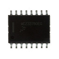
MCZ33780EG Freescale, MCZ33780EG Datasheet - Page 31

MCZ33780EG
Manufacturer Part Number
MCZ33780EG
Description
Manufacturer
Freescale
Datasheet
1.MCZ33780EG.pdf
(37 pages)
Specifications of MCZ33780EG
Operating Supply Voltage (typ)
5/12/15/18/24V
Operating Supply Voltage (min)
4.75/9V
Operating Supply Voltage (max)
5.25/25V
Operating Temp Range
-40C to 85C
Operating Temperature Classification
Industrial
Mounting
Surface Mount
Pin Count
16
Lead Free Status / RoHS Status
Compliant
Available stocks
Company
Part Number
Manufacturer
Quantity
Price
Company:
Part Number:
MCZ33780EG
Manufacturer:
Freescale Semiconductor
Quantity:
135
Company:
Part Number:
MCZ33780EG
Manufacturer:
Freescale
Quantity:
21
Part Number:
MCZ33780EG
Manufacturer:
FREESCALE
Quantity:
20 000
TSn – Indicates a Thermal Shutdown on Channel n
for a minimum of 16 clock cycles. The TSn bits are cleared
after a read of the DEN register if no longer in thermal
shutdown.
ENn – Controls Enabling and Disabling of Channel n
equation. Bit 7 represents x
Both the short and long word command use the same
polynomial. The polynomial bits beyond what is specified in
the CRCLEN[3:0] registers are ignored, and the most
significant term of each polynomial is assumed to be on. So,
for example, to represent a 6-bit CRC with a polynomial of
x
ignored in this case. These registers reset to 00010001 (x
1), which is the default DSI value (bit 4 does not need to be
on for this case but is included for readability).
seed for the CRC calculations. Both the short and long word
commands use the same seed. The seed bits beyond what is
specified in the CRCLEN[3:0] registers are ignored. So, for
example, to represent a 6-bit CRC with a seed 010101, the
value in DnSEED is xx010101. Bits 7 and 6 are ignored in this
case. These registers reset to 00001010, which is the default
DBUS value.
bus. Any bit changes will take place on the next DBUS
bus. Any bit changes will take place on the next DBUS
Analog Integrated Circuit Device Data
Freescale Semiconductor
6
SPI Data Bit
Read/Write
Reset
SPI Data Bit
Read/Write
Reset
SPI Data Bit
Read/Write
Reset
+ x
• 0 = No thermal shutdown occurring on Channel n.
• 1 = Thermal shutdown has occurred on Channel n.
The TSn bits are latched when a thermal shutdown occurs
• 0 = Channel n is disabled.
• 1 = Channel n is enabled.
Each bit represents a polynomial term in the CRC
The bits in these registers form a word that is used as the
A write to the register will abort any current activity on the
A write to the register will abort any current activity on the
3
+ 1, the value in DnPOLY is xx001001. Bits 7 and 6 are
CRCPOLY7 CRCPOLY6 CRCPOLY5 CRCPOLY4 CRCPOLY3 CRCPOLY2 CRCPOLY1 CRCPOLY0
CRCSEED7 CRCEED6
SWLEN3
Bit 7
Bit 7
Bit 7
0
0
1
Figure 32. Dn Short Word and CRC Length Register Bit Assignments
7
, bit 6 represents x
SWLEN2
6
0
6
0
6
0
Figure 30. Dn Polynomial Register Bit Assignments
Figure 31. Dn CRC Seed Register Bit Assignments
CRCEED5
SWLEN1
5
0
5
0
5
0
6
, and so on.
CRCEED4
SWLEN0
4
4
1
4
0
4
0
+
CRCEED3
CRCLEN3
thermal shutdown occurs. It is necessary to write a 1 to the
ENn bit to turn it back on.
DnPOLY REGISTERS
calculating the CRC that is transmitted/received on the DBUS
channels. There are two of these registers, one for each
DBUS channel. The bit assignments are shown in
bus. Any bit changes will take place on the next DBUS
transaction following the conclusion of the SPI write to the
register.
DnSEED REGISTERS
used for calculating the CRC that is transmitted/received on
the DBUS channels. There are two of these registers, one for
each DBUS channel. The bit assignments are shown in
Figure
transaction following the conclusion of the SPI write to the
register.
DnLENGTH REGISTERS
and CRC lengths for data that is transmitted/received on the
DBUS channels. There are two of these registers, one for
each DBUS channel. The bit assignments are shown in
Figure
transaction following the conclusion of the SPI write to the
register.
3
0
3
1
3
0
The ENn bits are cleared and the channel disabled if a
These read/write registers control the polynomial used for
A write to the register will abort any current activity on the
These read/write registers control the initial value, or seed,
These read/write registers control the short word lengths
31.
32.
CRCEED2
CRCLEN2
2
0
2
0
2
1
CRCEED1
CRCLEN1
LOGIC COMMANDS AND REGISTERS
1
0
1
1
1
0
FUNCTIONAL DEVICE OPERATION
CRCEED0
CRCLEN0
0
1
0
0
0
0
Figure
33780
30.
31


