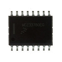
MCZ33780EG Freescale, MCZ33780EG Datasheet - Page 15

MCZ33780EG
Manufacturer Part Number
MCZ33780EG
Description
Manufacturer
Freescale
Datasheet
1.MCZ33780EG.pdf
(37 pages)
Specifications of MCZ33780EG
Operating Supply Voltage (typ)
5/12/15/18/24V
Operating Supply Voltage (min)
4.75/9V
Operating Supply Voltage (max)
5.25/25V
Operating Temp Range
-40C to 85C
Operating Temperature Classification
Industrial
Mounting
Surface Mount
Pin Count
16
Lead Free Status / RoHS Status
Compliant
Available stocks
Company
Part Number
Manufacturer
Quantity
Price
Company:
Part Number:
MCZ33780EG
Manufacturer:
Freescale Semiconductor
Quantity:
135
Company:
Part Number:
MCZ33780EG
Manufacturer:
Freescale
Quantity:
21
Part Number:
MCZ33780EG
Manufacturer:
FREESCALE
Quantity:
20 000
PROTOCOL ENGINE
registers into the DBUS sequences, and converts DBUS
response sequences to data in the registers. It generates the
proper DBUS timing.
DBUS DRIVER / RECEIVER (PHYSICAL LAYER)
current needed to drive the DBUS. It also detects the
response current from the slave devices and translates that
current into digital levels. These circuits can drive their
outputs to the levels listed in
state change, and internal signal DSIS controls the signal
level, high or low. DSIR is the slave device response signal to
the logic. This is shown in
Analog Integrated Circuit Device Data
Freescale Semiconductor
Table 6. Internal Signal Truth Table
This block converts the data to be transmitted from the
This block translates the transmit data to the voltage and
The internal signal DSIF controls the Idle to Signalling
DSIF
X
0
0
1
1
DSIR
DSIS
DSIF
DSIS
0
1
0
1
X
Overvoltage
T
LIM
0
0
0
0
1
Table
Generation
Differential
Control
Table
Signal
Return Data
Return Data
6.
DSIR
0
0
0
T
5.
LIM
Figure 10. Driver/Receiver Block Diagram
High Impedance
High Impedance
Signal High
Signal Low
Comp.
DnD
Idle
Signal
Signal
with a duty cycle determined by the logic state. The protocol
requires Cyclical Redundancy Check (CRC) generation and
validation.
circuit uses independent drivers for the Idle and Signal states.
This allows each driver to be optimized for its function. The
Idle driver is active in Idle and during the transitions from Idle
to Signal high and Signal high to Idle. The Signal driver is only
active during actual signaling. Both drivers are disabled in
HiZ.
recharge the Slave device storage capacitors. It is also
required to drive the DBUS load capacitances and control the
slew rate over a wide supply voltage range. The DnH and
DnL Idle drivers are each optimized for their specific drive
requirements.
and has the requirement of good slew rate control and
stability over a wide range of load conditions. The DnH and
DnL outputs use identical Signal driver circuits.
connected between each output and ground. These are the
DBUS common mode capacitors. In addition, a bypass
capacitor is required at V
located close to the IC pins and provide a low impedance
path to ground.
The DBUS transmit protocol uses a return to 1 type data
The DBUS driver block diagram is shown in
The Idle driver is required to supply a high current to
The Signal driver is optimized for driving the DBUS load,
To ensure stability of the Signal driver, capacitors must be
FUNCTIONAL INTERNAL BLOCK DESCRIPTION
Idle
Idle
SUP
Correction
. These capacitors must be
Common
Mode
FUNCTIONAL DESCRIPTIONS
Figure
DnH
DnL
10. The
33780
15


