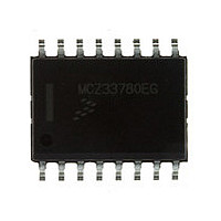
MCZ33780EG Freescale, MCZ33780EG Datasheet - Page 30

MCZ33780EG
Manufacturer Part Number
MCZ33780EG
Description
Manufacturer
Freescale
Datasheet
1.MCZ33780EG.pdf
(37 pages)
Specifications of MCZ33780EG
Operating Supply Voltage (typ)
5/12/15/18/24V
Operating Supply Voltage (min)
4.75/9V
Operating Supply Voltage (max)
5.25/25V
Operating Temp Range
-40C to 85C
Operating Temperature Classification
Industrial
Mounting
Surface Mount
Pin Count
16
Lead Free Status / RoHS Status
Compliant
Available stocks
Company
Part Number
Manufacturer
Quantity
Price
Company:
Part Number:
MCZ33780EG
Manufacturer:
Freescale Semiconductor
Quantity:
135
Company:
Part Number:
MCZ33780EG
Manufacturer:
Freescale
Quantity:
21
Part Number:
MCZ33780EG
Manufacturer:
FREESCALE
Quantity:
20 000
DnCTRL REGISTER
used on the DBUS. There are two of these registers, one for
register should be written to before data is sent over its bus.
A write to the register will abort any current activity on the bus.
Any bit changes will take place on the next DBUS transaction
following the conclusion of the SPI write to the register. Refer
to the
DLY[B:A]–Interframe Delay for Channel n
frames on the bus as illustrated in
when DLY[B:A] is set to 00, there is a minimum of four bit
times of IDLE voltage level. The time is measured from the
end of a DBUS transaction (signaled by the start of the signal
high to IDLE voltage transition) to the start of a new DBUS
transaction (signaled by the start of the IDLE voltage to signal
high transition).
Table 9. DLY[B:A] Frame Spacing
RIE–Receive Interrupt Enable Channel n
TIE–Transmit Interrupt Enable Channel n
30
33780
FUNCTIONAL DEVICE OPERATION
LOGIC COMMANDS AND REGISTERS
SPI Data Bit
Read/Write
Reset
SPI Data Bit
Read/Write
Reset
The read / write DnCTRL register sets up conditions to be
Each output n has an associated DnCTRL register. This
These bits specify the minimum delay between transfer
• 0 = Receive interrupt disabled. RFNE status does not
• 1 = Receive interrupt enabled. Whenever the RFNE
• 0 = Transmit interrupt disabled. TFE status does not
DLY[B:A]
affect
status flag is 1, the
interrupt.
affect
Protocol Engine
00
01
10
11
INT
INT
pin.
pin.
(Read-Only)
DIV1
Bit 7
Bit 7
TS1
0
0
section for more detail.
Minimum Delay Between Frames
INT
pin will be low to request an
(Read-Only)
DIV0
TS0
6
0
6
0
Table
(Bit Times)
Figure 28. Dn Control Register Bit Assignment
4
5
6
8
9. For example,
DLYB
5
0
5
0
0
Figure 29. DEN Register Bits
DLYA
4
0
0
4
0
Table 10. Clock Divider
each of the buses. The bit assignments are shown in
Figure
MS–Message Size for Channel n
of CRC. The Short Word can be made to have between 8 and
15 bits of data and 0 to 8 bits of CRC. Long words are
generally used for configuration and setup messages. Short
words are generally used for DBUS data transactions.
DIV[1:0]–Clock Divider
bit rate to be reduced by selectable integer values. The
divider values are shown in
used during fixed frequency operation and is ignored when in
the spread-spectrum mode.
DEN Register
of the busses. It also allows the state of the thermal
shutdowns to be read. The bit assignments are shown in
Figure
driver will be tri-stated and the receive current detector
disabled. This will result in an all 0 response, which will cause
a CRC error.
RIE
3
0
0
3
0
• 1 = Transmit interrupt enabled. Whenever the TFE
•0 = Long Word.
•1 = Short Word
The Long Word will contain 16 bits of data and 0 to 8 bits
The DIV bits set a pre-scaler for the bit clock to allow the
This read / write register is used to enable or disable each
status flag is 1, the
interrupt.
28.
29. If a thermal shutdown occurs, the output of the bus
2
0
0
TIE
2
0
DIV[1:0]
00
01
10
11
EN1
Analog Integrated Circuit Device Data
1
0
INT
1
0
0
Table
pin will be low to request an
EN0
10. The clock divider is
Freescale Semiconductor
0
0
MS
0
0
N
1
2
4
8


