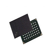
MT48LC16M16A2FG-75:D Micron Technology Inc, MT48LC16M16A2FG-75:D Datasheet - Page 56

MT48LC16M16A2FG-75:D
Manufacturer Part Number
MT48LC16M16A2FG-75:D
Description
DRAM Chip SDRAM 256M-Bit 16Mx16 3.3V 54-Pin VFBGA Tray
Manufacturer
Micron Technology Inc
Type
SDRAMr
Datasheet
1.MT48LC16M16A2FG-75D.pdf
(87 pages)
Specifications of MT48LC16M16A2FG-75:D
Density
256 Mb
Maximum Clock Rate
133 MHz
Package
54VFBGA
Address Bus Width
15 Bit
Operating Supply Voltage
3.3 V
Maximum Random Access Time
6|5.4 ns
Operating Temperature
0 to 70 °C
Organization
16Mx16
Address Bus
15b
Access Time (max)
6/5.4ns
Operating Supply Voltage (typ)
3.3V
Package Type
VFBGA
Operating Temp Range
0C to 70C
Operating Supply Voltage (max)
3.6V
Operating Supply Voltage (min)
3V
Supply Current
135mA
Pin Count
54
Mounting
Surface Mount
Operating Temperature Classification
Commercial
Lead Free Status / RoHS Status
Not Compliant
Available stocks
Company
Part Number
Manufacturer
Quantity
Price
Company:
Part Number:
MT48LC16M16A2FG-75:D TR
Manufacturer:
Micron Technology Inc
Quantity:
10 000
Figure 26: Terminating a READ Burst
PDF: 09005aef8091e6d1
256Mb_sdr.pdf - Rev. N 1/10 EN
Note:
Continuous-page READ bursts can be truncated with a BURST TERMINATE command
and fixed-length READ bursts can be truncated with a BURST TERMINATE command,
provided that auto precharge was not activated. The BURST TERMINATE command
should be issued x cycles before the clock edge at which the last desired data element is
valid, where x = CL - 1. This is shown in Figure 26 (page 56) for each possible CAS
latency; data element n + 3 is the last desired data element of a longer burst.
Command
Command
1. DQM is LOW.
Address
Address
CLK
CLK
DQ
DQ
Bank,
T0
Col n
T0
READ
Bank,
READ
Col n
CL = 2
CL = 3
T1
T1
NOP
NOP
56
T2
T2
NOP
NOP
D
OUT
Micron Technology, Inc. reserves the right to change products or specifications without notice.
T3
T3
NOP
NOP
D
D
OUT
OUT
TERMINATE
TERMINATE
BURST
BURST
T4
T4
X = 1 cycle
D
D
256Mb: x4, x8, x16 SDRAM
OUT
OUT
Transitioning data
X = 2 cycles
T5
T5
NOP
NOP
D
D
OUT
OUT
© 1999 Micron Technology, Inc. All rights reserved.
T6
T6
READ Operation
NOP
NOP
D
OUT
Don’t Care
T7
NOP


