BF996S,215 NXP Semiconductors, BF996S,215 Datasheet
BF996S,215
Specifications of BF996S,215


Related parts for BF996S,215


BF996S,215 Summary of contents
Page 1
DATA SHEET BF996S N-channel dual-gate MOS-FET Product specification DISCRETE SEMICONDUCTORS April 1991 ...
Page 2
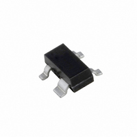
... NXP Semiconductors N-channel dual-gate MOS-FET FEATURES Protected against excessive input voltage surges by integrated back-to-back diodes between gates and source. APPLICATIONS RF applications such as: – UHF television tuners – Professional communication equipment. PINNING PIN SYMBOL source 2 d drain 3 g gate gate 1 ...
Page 3
... NXP Semiconductors N-channel dual-gate MOS-FET LIMITING VALUES In accordance with the Absolute Maximum Rating System (IEC 134). SYMBOL PARAMETER V drain-source voltage DS I drain current (DC average drain current D(AV) I gate 1 source G1-S I gate 2 source G1-S P total power dissipation tot T storage temperature range stg ...
Page 4
... NXP Semiconductors N-channel dual-gate MOS-FET STATIC CHARACTERISTICS = 25 C unless otherwise specified SYMBOL PARAMETER I gate cut-off current G1SS I gate cut-off current G2SS V gate-source breakdown voltage (BR)G1-SS V gate-source breakdown voltage (BR)G2-SS I drain current DSS V gate-source cut-off current (P)G1-S V gate-source cut-off current (P)G2-S DYNAMIC CHARACTERISTICS ...
Page 5
... NXP Semiconductors N-channel dual-gate MOS-FET PACKAGE OUTLINE Plastic surface-mounted package; 4 leads DIMENSIONS (mm are the original dimensions UNIT max 1.1 0.48 0.88 0.1 mm 0.9 0.38 0.78 OUTLINE VERSION IEC SOT143B April 1991 scale 0.15 3.0 1.4 1.9 1.7 0.09 2.8 1.2 REFERENCES ...
Page 6
... In no event shall NXP Semiconductors be liable for any indirect, incidental, punitive, special or consequential damages (including - without limitation - lost profits, lost savings, business interruption, costs related to the ...
Page 7
... NXP Semiconductors’ specifications such use shall be solely at customer’s own risk, and (c) customer fully indemnifies NXP Semiconductors for any liability, damages or failed product claims resulting from customer design and use of the product for automotive applications beyond NXP Semiconductors’ ...
Page 8
... Interface, Security and Digital Processing expertise Customer notification This data sheet was changed to reflect the new company name NXP Semiconductors, including new legal definitions and disclaimers. No changes were made to the technical content, except for package outline drawings which were updated to the latest version. ...