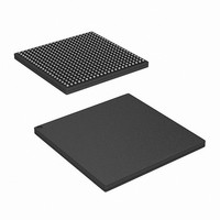
CYD18S72V-100BBC Cypress Semiconductor Corp, CYD18S72V-100BBC Datasheet - Page 9

CYD18S72V-100BBC
Manufacturer Part Number
CYD18S72V-100BBC
Description
IC,SYNC SRAM,256KX72,CMOS,BGA,484PIN,PLASTIC
Manufacturer
Cypress Semiconductor Corp
Datasheet
1.CYD09S72V-133BBC.pdf
(26 pages)
Specifications of CYD18S72V-100BBC
Format - Memory
RAM
Memory Type
SRAM - Dual Port, Synchronous
Memory Size
18M (256K x 72)
Speed
100MHz
Interface
Parallel
Voltage - Supply
3.135 V ~ 3.465 V
Operating Temperature
0°C ~ 70°C
Package / Case
484-FBGA
Lead Free Status / RoHS Status
Contains lead / RoHS non-compliant
Available stocks
Company
Part Number
Manufacturer
Quantity
Price
Company:
Part Number:
CYD18S72V-100BBC
Manufacturer:
Cypress Semiconductor Corp
Quantity:
10 000
IEEE 1149.1 Serial Boundary Scan (JTAG)
The FLEx72 incorporates an IEEE 1149.1 serial boundary scan
test access port (TAP). The TAP controller functions in a manner
that does not conflict with the operation of other devices using
1149.1-compliant TAPs. The TAP operates using
JEDEC-standard 3.3 V I/O logic levels. It is composed of three
input connections and one output connection required by the test
logic defined by the standard.
Performing a TAP Reset
A reset is performed by forcing TMS HIGH (V
edges of TCK. This reset does not affect the operation of the
FLEx72 family and may be performed while the device is
operating. An MRST must be performed on the FLEx72 after
power-up.
Performing a Pause/Restart
When a SHIFT-DR PAUSE-DR SHIFT-DR is performed the scan
chain will output the next bit in the chain twice. For example, if
the value expected from the chain is 1010101, the device will
output a 11010101. This extra bit will cause some testers to
report an erroneous failure for the FLEx72 in a scan test.
Therefore the tester should be configured to never enter the
PAUSE-DR state.
Notes
Document Number : 38-06069 Rev. *K
19. The “X” in this diagram represents the counter upper bits.
20. Boundary scan is IEEE 1149.1-compatible. See “Performing a Pause/Restart” for deviation from strict 1149.1 compliance.
Figure 2. Programmable Counter-Mask Register Operation
Example:
Load
Counter-Mask
Register = 3F
Load
Address
Counter = 8
Max + 1
Address
Register
Max
Address
Register
CNTINT
H
H
L
H
DD
) for five rising
2
2
2
2
16
16
16
16
X
0
X
X
2
2
2
2
15
15
15
15
X
0
X
X
Masked Address
[20]
[1, 19]
Xs
0s
Xs
Xs
Boundary Scan Hierarchy for FLEx72 Family
Internally, the CYD04S72V and CYD09S72V have two DIEs
while CYD18S72V have four DIEs. Each DIE contains all the
circuitry required to support boundary scan testing. The circuitry
includes the TAP, TAP controller, instruction register, and data
registers. The circuity and operation of the DIE boundary scan
are described in detail below. The scan chain of each DIE is
connected serially to form the scan chain of the FLEx72 family
as shown in
each DIE to drive all 4 TAP controllers in unison. In many cases,
each DIE will be supplied with the same instruction. In other
cases, it might be useful to supply different instructions to each
DIE. One example would be testing the device ID of one DIE
while bypassing the others.
Each pin of FLEx72 family is typically connected to multiple DIEs.
For connectivity testing with the EXTEST instruction, it is
desirable to check the internal connections between DIEs as well
as the external connections to the package. This can be
accomplished by merging the netlist of the devices with the
netlist of the user’s circuit board. To facilitate boundary scan
testing of the devices, Cypress provides the BSDL file for each
DIE, the internal netlist of the device, and a description of the
device scan chain. The user can use these materials to easily
integrate the devices into the board’s boundary scan
environment. Further information can be found in the Cypress
application note Using JTAG Boundary Scan For System In a
Package (SIP) Dual-Port SRAMs.
2
2
2
2
6
6
6
6
X
0
X
X
2
2
2
2
Figure
5
5
5
5
0 0
1 1
0 0
1 1
Unmasked Address
2
2
2
2
4
4
4
4
2
2
2
2
3. TMS and TCK are connected in parallel to
3
3
3
3
1
1
1
1
2
2
2
2
2
2
2
2
0
1
0
1
2
2
2
2
1
1
1
1
0
1
0
1
2
2
2
2
0
0
0
0
0
1
0
1
Mask
Register
bit-0
Address
Counter
bit-0
CYD04S72V
CYD09S72V
CYD18S72V
Page 9 of 26
[+] Feedback


