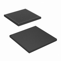
CYD18S72V-100BBC Cypress Semiconductor Corp, CYD18S72V-100BBC Datasheet - Page 16

CYD18S72V-100BBC
Manufacturer Part Number
CYD18S72V-100BBC
Description
IC,SYNC SRAM,256KX72,CMOS,BGA,484PIN,PLASTIC
Manufacturer
Cypress Semiconductor Corp
Datasheet
1.CYD09S72V-133BBC.pdf
(26 pages)
Specifications of CYD18S72V-100BBC
Format - Memory
RAM
Memory Type
SRAM - Dual Port, Synchronous
Memory Size
18M (256K x 72)
Speed
100MHz
Interface
Parallel
Voltage - Supply
3.135 V ~ 3.465 V
Operating Temperature
0°C ~ 70°C
Package / Case
484-FBGA
Lead Free Status / RoHS Status
Contains lead / RoHS non-compliant
Available stocks
Company
Part Number
Manufacturer
Quantity
Price
Company:
Part Number:
CYD18S72V-100BBC
Manufacturer:
Cypress Semiconductor Corp
Quantity:
10 000
Switching Waveforms
Bank Select Read
Notes
Document Number : 38-06069 Rev. *K
ADDRESS
ADDRESS
Read-to-Write-to-Read (OE = LOW)
33. In this depth-expansion example, B1 represents Bank #1 and B2 is Bank #2; each bank consists of one Cypress FLEx72 device from this data sheet. ADDRESS
34. ADS = CNTEN = BE0 – BE7 = OE = LOW; MRST = CNTRST = CNT/MSK = HIGH.
35. Output state (HIGH, LOW, or high-impedance) is determined by the previous cycle control signals.
36. During “No Operation,” data in memory at the selected address may be corrupted and should be rewritten to ensure data integrity.
37. CE
38. CE
DATA
DATA
ADDRESS
DATA
= ADDRESS
completed (labelled as no operation). One clock cycle is required to three-state the I/O for the Write operation on the next rising edge of CLK.
DATA
0
0
OUT(B2)
OUT(B1)
CE
CE
= BE0 – BE7 = R/W = LOW; CE
CLK
R/W
= OE = BE0 – BE7 = LOW; CE
OUT
CE
CLK
(B1)
(B1)
(B2)
IN
(B2)
(B2)
t
t
t
SW
SC
SA
.
t
t
t
t
SA
SC
SA
SC
[33, 34]
A
n
A
A
t
0
0
CH2
t
CH2
t
CYC2
t
t
t
HW
HC
HA
t
1
t
t
t
t
CYC2
1
HC
HC
HA
HA
(continued)
= R/W = CNTRST = MRST = HIGH.
= CNTRST = MRST = CNT/MSK = HIGH. When R/W first switches low, since OE = LOW, the Write operation cannot be
t
CL2
t
CL2
READ
A
n+1
A
A
[32, 35, 36, 37, 38]
t
CD2
1
1
t
CD2
t
SW
t
Q
SC
n
Q
t
A
0
SC
n+2
t
A
DC
A
2
2
t
t
DC
HC
t
HW
t
HC
t
CD2
NO OPERATION
A
n+2
Q
A
t
A
1
CKHZ
3
t
3
DC
t
t
CKLZ
CKHZ
t
CD2
t
SD
D
A
n+2
n+2
Q
A
A
t
HD
4
2
4
t
t
t
CKHZ
CD2
CKLZ
WRITE
Q
3
A
CYD04S72V
CYD09S72V
CYD18S72V
n+3
A
A
5
t
5
CKLZ
t
t
CKHZ
CD2
Page 16 of 26
(B1)
Q
4
[+] Feedback


