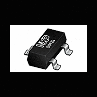
PESD36VS2UT NXP Semiconductors, PESD36VS2UT Datasheet - Page 7

PESD36VS2UT
Manufacturer Part Number
PESD36VS2UT
Description
DIODE,DUAL ESD TVS,UNI DIR,36V,SOT23
Manufacturer
NXP Semiconductors
Datasheet
1.PESD36VS2UT215.pdf
(12 pages)
Specifications of PESD36VS2UT
Reverse Stand-off Voltage Vrwm
36V
Breakdown Voltage Range
40V
Clamping Voltage Vc Max
60V
Diode Configuration
Common Anode
Peak Pulse Current Ippm
2.5A
Diode Case Style
SOT-23
No. Of
RoHS Compliant
Available stocks
Company
Part Number
Manufacturer
Quantity
Price
Company:
Part Number:
PESD36VS2UT
Manufacturer:
NXP
Quantity:
42 000
Part Number:
PESD36VS2UT
Manufacturer:
NXP/恩智浦
Quantity:
20 000
Part Number:
PESD36VS2UT,215
Manufacturer:
NEXPERIA/安世
Quantity:
20 000
NXP Semiconductors
7. Application information
8. Test information
PESD36VS2UT_1
Product data sheet
8.1 Quality information
The PESD36VS2UT is designed for the protection of up to two unidirectional data or
signal lines from the damage caused by ESD and surge pulses. The devices may be used
on lines where the signal polarities are either positive or negative with respect to ground.
The PESD36VS2UT provides a surge capability of 160 W per line for an 8/20 s
waveform.
Circuit board layout and protection device placement
Circuit board layout is critical for the suppression of ESD, Electrical Fast Transient (EFT)
and surge transients. The following guidelines are recommended:
This product has been qualified in accordance with the Automotive Electronics Council
(AEC) standard Q101 - Stress test qualification for discrete semiconductors , and is
suitable for use in automotive applications.
1. Place the device as close to the input terminal or connector as possible.
2. The path length between the device and the protected line should be minimized.
3. Keep parallel signal paths to a minimum.
4. Avoid running protected conductors in parallel with unprotected conductors.
5. Minimize all Printed-Circuit Board (PCB) conductive loops including power and
6. Minimize the length of the transient return path to ground.
7. Avoid using shared transient return paths to a common ground point.
8. Ground planes should be used whenever possible. For multilayer PCBs, use ground
Fig 7.
ground loops.
vias.
Application diagram
unidirectional protection
Rev. 01 — 16 July 2009
Low capacitance unidirectional double ESD protection diode
of two lines
line 1 to be protected
line 2 to be protected
PESD36VS2UT
GND
bidirectional protection
of one line
PESD36VS2UT
line 1 to be protected
GND
PESD36VS2UT
006aab617
© NXP B.V. 2009. All rights reserved.
7 of 12


