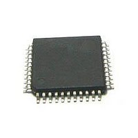
MC56F8255VLD Freescale Semiconductor, MC56F8255VLD Datasheet - Page 49

MC56F8255VLD
Manufacturer Part Number
MC56F8255VLD
Description
DSC 64K FLASH 60MHZ 44-LQFP
Manufacturer
Freescale Semiconductor
Series
56F8xxxr
Datasheets
1.TWR-56F8257.pdf
(88 pages)
2.MC56F8245VLD.pdf
(14 pages)
3.MC56F8245VLD.pdf
(2 pages)
4.MC56F8245VLD.pdf
(629 pages)
Specifications of MC56F8255VLD
Core Processor
56800E
Core Size
16-Bit
Speed
60MHz
Connectivity
CAN, I²C, LIN, SCI, SPI
Peripherals
LVD, POR, PWM, WDT
Number Of I /o
35
Program Memory Size
64KB (32K x 16)
Program Memory Type
FLASH
Ram Size
4K x 16
Voltage - Supply (vcc/vdd)
3 V ~ 3.6 V
Data Converters
A/D 8x12b, D/A 1x12b
Oscillator Type
Internal
Operating Temperature
-40°C ~ 105°C
Package / Case
44-LQFP
Product
DSCs
Processor Series
56800E
Core
56800E
Device Million Instructions Per Second
60 MIPs
Maximum Clock Frequency
60 MHz
Number Of Programmable I/os
35
Data Ram Size
8 KB
Operating Supply Voltage
3.3 V
Maximum Operating Temperature
+ 105 C
Mounting Style
SMD/SMT
Minimum Operating Temperature
- 40 C
On-chip Adc
12 bit, 4 Channel
Lead Free Status / RoHS Status
Lead free / RoHS Compliant
Eeprom Size
-
Lead Free Status / Rohs Status
Details
Available stocks
Company
Part Number
Manufacturer
Quantity
Price
Company:
Part Number:
MC56F8255VLD
Manufacturer:
Freescale Semiconductor
Quantity:
10 000
7.2
Absolute maximum ratings are stress ratings only, and functional operation at the maximum is not guaranteed.
Unless otherwise stated, all specifications within this section apply over the ambient temperature range of –40 ºC to +105 ºC
over the following supply ranges: V
For functional operating conditions, refer to the remaining tables in the section.
1
Default Mode
Pin Group 1: GPIO, TDI, TDO, TMS, TCK
Pin Group 2: RESET, GPIOA7
Pin Group 3: ADC and Comparator Analog Inputs
Pin Group 4: XTAL, EXTAL
Pin Group 5: DAC analog output
Freescale Semiconductor
Supply Voltage Range
Analog Supply Voltage Range
ADC High Voltage Reference
Voltage difference V
Voltage difference V
Digital Input Voltage Range
Oscillator Voltage Range
Analog Input Voltage Range
Input clamp current, per pin (V
Output clamp current, per pin (V
Output Voltage Range
(Normal Push-Pull mode)
Output Voltage Range
(Open Drain mode)
DAC Output Voltage Range
Ambient Temperature
Industrial
Storage Temperature Range
(Extended Industrial)
Continuous clamp current per pin is –2.0 mA
Absolute Maximum Ratings
Characteristic
Stress beyond the limits specified in
permanent damage to the device.
DD
SS
to V
to V
SSA
DDA
Table 17. Absolute Maximum Ratings
IN
O
< 0)
MC56F825x/MC56F824x Digital Signal Controller, Rev. 3
< 0)
SS
1
1
= V
SSA
= 0 V, V
V
Symbol
V
V
OUT_DAC
V
V
V
OUTOD
T
V
V
REFHx
V
Table 17
V
V
V
V
DD
OSC
OUT
T
STG
DDA
INA
OC
CAUTION
DD
IN
IC
A
DD
SS
= V
DDA
may affect device reliability or cause
= 3.0 V to 3.6 V, CL < 50 pF, f
Pin Groups 1, 2
Pin Group 4
Pin Group 3
Pin Group 1
Pin Group 2
Pin Group 5
Notes
(V
SS
= 0 V, V
SSA
- 0.3
- 0.3
- 0.3
- 0.3
- 0.3
- 0.3
- 0.4
- 0.3
- 0.3
- 0.3
- 0.3
= 0 V)
Min
- 40
- 55
—
—
OP
= 60 MHz.
-20.0
-20.0
Max
105
150
4.0
4.0
4.0
0.3
0.3
6.0
4.0
4.0
4.0
6.0
4.0
Specifications
Unit
mA
mA
°C
°C
V
V
V
V
V
V
V
V
V
V
V
49


