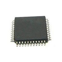
MC56F8255VLD Freescale Semiconductor, MC56F8255VLD Datasheet - Page 18

MC56F8255VLD
Manufacturer Part Number
MC56F8255VLD
Description
DSC 64K FLASH 60MHZ 44-LQFP
Manufacturer
Freescale Semiconductor
Series
56F8xxxr
Datasheets
1.TWR-56F8257.pdf
(88 pages)
2.MC56F8245VLD.pdf
(14 pages)
3.MC56F8245VLD.pdf
(2 pages)
4.MC56F8245VLD.pdf
(629 pages)
Specifications of MC56F8255VLD
Core Processor
56800E
Core Size
16-Bit
Speed
60MHz
Connectivity
CAN, I²C, LIN, SCI, SPI
Peripherals
LVD, POR, PWM, WDT
Number Of I /o
35
Program Memory Size
64KB (32K x 16)
Program Memory Type
FLASH
Ram Size
4K x 16
Voltage - Supply (vcc/vdd)
3 V ~ 3.6 V
Data Converters
A/D 8x12b, D/A 1x12b
Oscillator Type
Internal
Operating Temperature
-40°C ~ 105°C
Package / Case
44-LQFP
Product
DSCs
Processor Series
56800E
Core
56800E
Device Million Instructions Per Second
60 MIPs
Maximum Clock Frequency
60 MHz
Number Of Programmable I/os
35
Data Ram Size
8 KB
Operating Supply Voltage
3.3 V
Maximum Operating Temperature
+ 105 C
Mounting Style
SMD/SMT
Minimum Operating Temperature
- 40 C
On-chip Adc
12 bit, 4 Channel
Lead Free Status / RoHS Status
Lead free / RoHS Compliant
Eeprom Size
-
Lead Free Status / Rohs Status
Details
Available stocks
Company
Part Number
Manufacturer
Quantity
Price
Company:
Part Number:
MC56F8255VLD
Manufacturer:
Freescale Semiconductor
Quantity:
10 000
Signal/Connection Descriptions
3.3
After reset, each pin is configured for its primary function (listed first). Any alternative functionality, shown in parentheses and
as italic, must be programmed via the GPIO module’s peripheral enable registers (GPIO_x_PER) and the SIM module’s GPIO
peripheral select (GPSx) registers.
18
(GPIOD0)
(GPIOD1)
(GPIOD2)
Signal
Name
V
V
V
V
TDO
TCK
V
V
V
V
V
V
TDI
DDA
SSA
CAP
CAP
DD
DD
DD
SS
SS
SS
MC56F825x/MC56F824x Signal Pins
LQFP
44
29
40
20
28
41
13
14
17
39
44
42
1
LQFP
48
32
44
22
31
45
15
16
19
43
48
46
1
Table 5. MC56F825x/MC56F824x Signal and Package Information
LQFP
64
29
44
60
30
43
61
22
23
26
57
64
62
1
MC56F825x/MC56F824x Digital Signal Controller, Rev. 3
Supply
Supply
Supply
Supply
Supply
Output
Output
Output
Output
Input/
Input/
Input/
Type
Input
Input
enabled
enabled
internal
internal
During
Supply
Supply
Supply
Supply
Supply
Output
Reset
pullup
pullup
Input,
Input,
State
I/O Power — This pin supplies 3.3 V power to the chip I/O interface.
I/O Ground — These pins provide ground for chip I/O interface.
Analog Power — This pin supplies 3.3 V power to the analog
modules. It must be connected to a clean analog power supply.
Analog Ground — This pin supplies an analog ground to the analog
modules. It must be connected to a clean power supply.
V
this pin and V
required for proper device operation. See
Design
Test Data Input — This input pin provides a serial input data stream
to the JTAG/EOnCE port. It is sampled on the rising edge of TCK
and has an on-chip pullup resistor.
Port D GPIO — This GPIO pin can be individually programmed as
an input or output pin.
After reset, the default state is TDI.
Test Data Output — This tri-stateable output pin provides a serial
output data stream from the JTAG/EOnCE port. It is driven in the
shift-IR and shift-DR controller states, and changes on the falling
edge of TCK.
Port D GPIO — This GPIO pin can be individually programmed as
an input or output pin.
After reset, the default state is TDO.
Test Clock Input — This input pin provides a gated clock to
synchronize the test logic and shift serial data to the JTAG/EOnCE
port. The pin is connected internally to a pullup resistor. A
Schmitt-trigger input is used for noise immunity.
Port D GPIO — This GPIO pin can be individually programmed as
an input or output pin.
After reset, the default state is TCK
CAP
— Connect a bypass capacitor of 2.2 µF or greater between
Considerations,”
SS
to stabilize the core voltage regulator output
Signal Description
on page
73.
Freescale Semiconductor
Section 8.2, “Electrical


