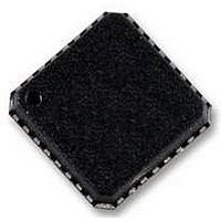
AD9553BCPZ Analog Devices Inc, AD9553BCPZ Datasheet - Page 40

AD9553BCPZ
Manufacturer Part Number
AD9553BCPZ
Description
IC INTEGER-N CLCK GEN 32LFCSP
Manufacturer
Analog Devices Inc
Datasheet
1.AD9553PCBZ.pdf
(44 pages)
Specifications of AD9553BCPZ
Clock Ic Type
PLL Clock Driver
Ic Interface Type
3 Wire, Serial
Frequency
710MHz
No. Of Outputs
2
Supply Current
162mA
Supply Voltage Range
0V To 3.3V
Digital Ic Case Style
LFCSP
Lead Free Status / RoHS Status
Lead free / RoHS Compliant
Available stocks
Company
Part Number
Manufacturer
Quantity
Price
Company:
Part Number:
AD9553BCPZ
Manufacturer:
ADI
Quantity:
154
AD9553
OUT1 Driver Control (Register 0x32)
Table 37.
Address
0x32
Reserved (Register 0x33)
Table 38.
Address
0x33
Bit
7
6
[5:3]
2
1
0
Bit
[7:0]
Bit Name
OUT1 drive strength
OUT1 power-down
OUT1 mode control
OUT1 CMOS polarity
Unused
OUT1 mode source
Bit Name
Unused
Description
Unused.
Description
Controls the output drive capability of the OUT1 driver.
0 = weak.
1 = strong (default).
Controls power-down functionality of the OUT1 driver.
0 = OUT1 active (default).
1 = OUT1 powered down.
OUT1 driver mode selection.
000 = CMOS, both pins active.
001 = CMOS, positive pin active, negative pin tristate.
010 = CMOS, positive pin tristate, negative pin active.
011 = CMOS, both pins tristate.
100 = LVDS.
101 = LVPECL (default).
110 = not used.
111 = not used.
Selects the polarity of the OUT1 pins in CMOS mode. This bit is ineffective unless Bits[5:3]
select CMOS mode. See the Output Driver Polarity (CMOS) section for the definition of
normal and inverted polarity.
0 = positive pin is normal polarity and negative pin is normal polarity (default).
1 = positive pin logic is inverted polarity and negative pin is normal polarity.
Unused.
Controls OUT1 driver functionality (see Figure 31).
0 = OUT1 mode determined by the OM2 to OM0 pins (default).
1 = OUT1 mode defined by Register 0x32[5:3].
Rev. A | Page 40 of 44


