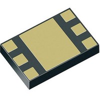
BGB 717L7ESD E6327 Infineon Technologies, BGB 717L7ESD E6327 Datasheet - Page 12

BGB 717L7ESD E6327
Manufacturer Part Number
BGB 717L7ESD E6327
Description
RF Bipolar Small Signal RF BIP TRANSISTORS
Manufacturer
Infineon Technologies
Datasheet
1.BGB_717L7ESD_E6433.pdf
(14 pages)
Specifications of BGB 717L7ESD E6327
Minimum Operating Temperature
- 55 C
Mounting Style
SMD/SMT
Maximum Operating Temperature
+ 150 C
Package / Case
TSLP-7-1
Lead Free Status / RoHS Status
Lead free / RoHS Compliant
Other names
BGB717L7ESDE6327XT
Table 6
Component
C
C
C
C
R
R
L
The following table gives an overview on the performance of the FM radio LNA application circuit. All data were
measured in a 50 Ω system.
Table 7
Parameter
Insertion power gain
Input return loss
Output return loss
Noise figure
Input 1dB gain compression point
Input 3
1) As described in AN176,
2) Verified by random sampling
3) High LNA input impedance leads to power matching with high ohmic antennas
4) Output matching is accomplished by the external resistors R1 and R2
5) An aggressive low pass filter prevents radio broadcast signals from distorting the NF measurement
Data Sheet
1
1
2
3
4
1
2
rd
Order Intercept Point
5)
Bill of Material
AC Characteristics in the FM Radio LNA Application
2)
2)
T
Value
330 pF
47 nF
47 nF
330 pF
56 Ω
10 Ω
470 nH
A
= 25°C,
2)
2)
V
CC
= 3 V,
Symbol
|
RL
RL
F
IP
IIP
S
50Ω
21
-1dB
IN
OUT
3
|
2
V
ctrl
= 3 V,
Min.
10
0
13
–
-8.0
-15.5
Manufacturer / Type
Various / 0402
Various / 0402
Various / 0402
Various / 0402
Various / 0402
Various / 0402
Taiyo Yuden LK1608R47K-T /
0603
12
I
CC
= 3 mA,
Typ.
12
0.5
16
1.0
-5.5
-12.5
Values
4)
3)
f
= 100 MHz
1)
Max.
14
3
19
1.5
–
–
Unit
dB
dB
dB
dB
dBm
dBm
DC blocking
DC stabilization
DC stabilization
DC blocking
matching and stabilization
stabilization
RF choke
Electrical Characteristics
Function
For biasing, output
For output matching and
Revision 3.3, 2010-06-24
Note /
Test Condition
–
–
–
Z
–
P
s
RFIN
BGB717L7ESD
= 50 Ω
= -40 dBm


