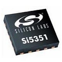
Si5351A-A-GM Silicon Laboratories Inc, Si5351A-A-GM Datasheet - Page 4

Si5351A-A-GM
Manufacturer Part Number
Si5351A-A-GM
Description
Clock Generators & Support Products AnyRate 2 PLL 125MHz Clk&I2C 8out
Manufacturer
Silicon Laboratories Inc
Type
Any Frequency CMOS Clock Generatorr
Specifications of Si5351A-A-GM
Mounting Style
SMD/SMT
Max Input Freq
0.008 MHz
Max Output Freq
133 MHz
Number Of Outputs
8
Operating Supply Voltage
3.3 V
Operating Temperature Range
- 40 C to + 85 C
Supply Current
25 mA
Package / Case
QFN-20
Lead Free Status / RoHS Status
Lead free / RoHS Compliant
Si5351A/B/C
1. Electrical Specifications
Table 1. Recommended Operating Conditions
Table 2. DC Characteristics
(V
4
Parameter
Ambient Temperature
Core Supply Voltage
Output Buffer Voltage
Notes:All minimum and maximum specifications are guaranteed and apply across the recommended operating conditions.
Parameter
Core Supply Current
Output Buffer Supply Current
(Per Output)*
Input Current
Output Impedance
*Note: Output clocks less than or equal to 100 MHz.
DD
= 2.5 V ±10%, or 3.3 V ±10%, T
Typical values apply at nominal supply voltages and an operating temperature of 25 °C unless otherwise noted.
VDD and VDDOx can be operated at independent voltages.
Power supply sequencing for VDD and VDDOx requires that both voltage rails are powered at the same time.
Symbol
V
V
DDOx
T
A
DD
A
= –40 to 85 °C)
Symbol
I
I
CLKIN
DDOx
I
I
Z
DD
VC
O
Test Condition
Preliminary Rev. 0.95
Power Down (PDN = V
8 mA output drive current.
See "6. Design Consider-
ations" on page 21.
Enabled 3 outputs
Enabled 8 outputs
CLKIN, SDA, SCL
Test Condition
Vin < 3.6 V
C
L
= 5 pF
VC
2.25
1.71
2.25
Min
–40
3.0
3.0
DD
)
Typ
3.3
2.5
1.8
2.5
3.3
Min
25
—
—
—
—
—
—
—
Typ
2.2
22
27
85
—
—
—
Max
3.60
2.75
1.89
2.75
3.60
85
Max
35
45
20
10
30
—
5
Unit
°C
Unit
V
V
V
V
V
mA
mA
mA
µA
µA
µA


