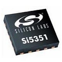
Si5351A-A-GM Silicon Laboratories Inc, Si5351A-A-GM Datasheet - Page 11

Si5351A-A-GM
Manufacturer Part Number
Si5351A-A-GM
Description
Clock Generators & Support Products AnyRate 2 PLL 125MHz Clk&I2C 8out
Manufacturer
Silicon Laboratories Inc
Type
Any Frequency CMOS Clock Generatorr
Specifications of Si5351A-A-GM
Mounting Style
SMD/SMT
Max Input Freq
0.008 MHz
Max Output Freq
133 MHz
Number Of Outputs
8
Operating Supply Voltage
3.3 V
Operating Temperature Range
- 40 C to + 85 C
Supply Current
25 mA
Package / Case
QFN-20
Lead Free Status / RoHS Status
Lead free / RoHS Compliant
3. Functional Description
The Si5351 is a versatile I
oscillators, VCXOs, PLLs, and buffers. A block diagram showing the general architecture of the Si5351 is shown in
Figure 3. The device consists of an input stage, two synthesis stages, and an output stage.
The input stage accepts an external crystal (XTAL), a clock input (CLKIN), or a control voltage input (VC)
depending on the version of the device (A/B/C). The first stage of synthesis multiplies the input frequencies to an
high-frequency intermediate clock, while the second stage of synthesis uses high resolution MultiSynth fractional
dividers to generate the desired output frequencies. Additional integer division is provided at the output stage for
generating output frequencies as low as 8 kHz. Crosspoint switches at each of the synthesis stages allows total
flexibility in routing any of the inputs to any of the outputs.
Because of this high resolution and flexible synthesis architecture, the Si5351 is capable of generating
synchronous or free-running non-integer related clock frequencies at each of its outputs, enabling one device to
synthesize clocks for multiple clock domains in a design.
3.1. Input Stage
3.1.1. Crystal Inputs (XA, XB)
The Si5351 uses a fixed-frequency standard AT-cut crystal as a reference to the internal oscillator. The output of
the oscillator can be used to provide a free-running reference to one or both of the PLLs for generating
asynchronous clocks. The output frequency of the oscillator will operate at the crystal frequency, either 25 MHz or
27 MHz. The crystal is also used as a reference to the VCXO to help maintain its frequency accuracy.
Internal load capacitors (C
to the Si5351. Options for internal load capacitors are 6, 8, or 10 pF. Crystals with alternate load capacitance
requirements are supported using additional external load capacitors as shown in Figure 4. Refer to application
note AN551 for crystal recommendations.
XTAL
CLKIN
VC
XA
XB
Stage
Input
VCXO
OSC
Div
Figure 4. External XTAL with Optional Load Capacitors
L
) are provided to eliminate the need for external components when connecting a crystal
2
C programmable clock generator that is ideally suited for replacing crystals, crystal
Synthesis
Stage 1
Figure 3. Si5351 Block Diagram
(VCXO)
PLL A
PLL B
(SSC)
Additional external
load capacitors
Optional
(< 2 pF)
C
C
L
L
Preliminary Rev. 0.95
XB
XA
C
L
Synthesis
Stage 2
Synth
Synth
Synth
Synth
Synth
Synth
Synth
Synth
Multi
Multi
Multi
Multi
Multi
Multi
Multi
Multi
C
0
1
2
3
4
5
6
7
L
Selectable internal
6 pF, 8 pF, 10 pF
load capacitors
R0
R1
R2
R3
R4
R5
R6
R7
Output
Stage
Si5351A/B/C
VDDOA
CLK0
CLK1
VDDOB
CLK2
CLK3
VDDOC
CLK4
CLK5
VDDOD
CLK6
CLK7
11


