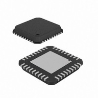
AT88RF1354-ZU Atmel, AT88RF1354-ZU Datasheet - Page 36

AT88RF1354-ZU
Manufacturer Part Number
AT88RF1354-ZU
Description
IC RF READER 13.56MHZ 36-VQFN
Manufacturer
Atmel
Datasheet
1.AT88RF1354-ZU.pdf
(48 pages)
Specifications of AT88RF1354-ZU
Frequency
13.56MHz
Features
ISO14443-B
Package / Case
36-VQFN Exposed Pad, 36-HVQFN, 36-SQFN, 36-DHVQFN
Pin Count
36
Screening Level
Industrial
Lead Free Status / RoHS Status
Lead free / RoHS Compliant
Rf Type
-
Lead Free Status / Rohs Status
Compliant
D.4.2. Stencil Design for Thermal Pad
D.4.3. Via Types and Solder Voiding
36
In order to effectively remove the heat from the package and to enhance the electrical performance, the die paddle
needs to be soldered to the PCB thermal pad, preferably with minimum voids. However, eliminating voids may not be
possible because of the presence of thermal vias and the large size of the thermal pad for larger size packages. Also,
out gassing occurs during the reflow process which may cause defects (splatter, solder balling) if the solder paste
coverage is too big. Therefore, it is recommended that smaller multiple openings in the stencil should be used instead
of one big opening for printing the solder paste on the thermal pad region. This will typically result in 50 to 80% solder
paste coverage. As shown in Figure D-3. some of the ways to achieve these levels of coverage.
Figure D-3. Thermal pad stencil design for 7x7 mm and 10x10 QFN packages
Voids within the solder joints under the exposed pad can have an adverse effect on high speed and RF applications as
well as on the thermal performance. As the QFN package incorporates a large center pad, controlling solder voiding
within this region can be difficult. Voids within this ground plane can increase the current path of the circuit. The
maximum size for a void should be less than the via pitch within the plane. This recommendation would assure that any
via would not be rendered ineffectual based on any void increasing the current path beyond the distance to the next
available via.
With regards to the voids in the thermal pad region, it should be emphasized that the presence of these voids is not
expected to result in degradation of the thermal and the electrical performance. No loss in thermal performance is
predicted from the thermal simulation of the smaller multiple voids covering up to 50% of the thermal pad area. It
should also be noted that voids in the thermal pad region do not impact the reliability of the perimeter solder joints.
Although the percentage of voids may not be a big concern, large voids in the thermal pad area should be avoided. In
order to control these voids, solder masking may be required for the thermal vias to prevent solder wicking inside the
via during reflow, thus displacing the solder away from the interface between the package die paddle and the thermal
pad on the PCB. There are different methods employed within the industry for this purpose, such as “via tenting” (from
the top or bottom side) using dry film solder mask, “via plugging” with liquid photoimagible (LPI) solder mask from the
bottom side, or “via encroaching”. These options are depicted in Figure D-4. In case of via tenting, the solder mask
diameter should be 100 microns larger than the via diameter.
13.56 MHz Type B RF Reader Specification
1.5 mm Dia. Circles
@ 1.6 mm Pitch
Coverage: 37%
1.35 x 1.35 mm Squares
@ 1.65 mm Pitch
Coverage: 68%
1.0 mm Dia. Circles
@ 1.2 mm Pitch
@ 1.2 mm Pitch
Coverage: 50%
1.35 x 1.35mm Squares
@ 1.5 mm Pitch
Coverage: 81%
8547B–RFID–3/09


