AT88RF1354-ZU Atmel, AT88RF1354-ZU Datasheet - Page 12
AT88RF1354-ZU
Manufacturer Part Number
AT88RF1354-ZU
Description
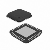
IC RF READER 13.56MHZ 36-VQFN
Manufacturer
Atmel
Datasheet
1.AT88RF1354-ZU.pdf
(48 pages)
Specifications of AT88RF1354-ZU
Frequency
13.56MHz
Features
ISO14443-B
Package / Case
36-VQFN Exposed Pad, 36-HVQFN, 36-SQFN, 36-DHVQFN
Pin Count
36
Screening Level
Industrial
Lead Free Status / RoHS Status
Lead free / RoHS Compliant
Rf Type
-
Lead Free Status / Rohs Status
Compliant


4.2.8. SDO [19]
4.2.9. SSB [13]
4.3.
4.3.1. ANT [3]
4.3.2. C6 [35]
4.3.3. RFin [32]
4.4.
4.4.1. C1 [21]
4.4.2. C2 [26]
4.4.3. C3 [27]
4.4.4. C4 [25]
4.4.5. C5 [6]
12
Serial Data Out pin. In SPI communication mode this pin functions as the serial data output. In TWI communication
mode this pin is not used.
SPI Slave Select Bar input pin. In SPI communication mode this pin functions as the slave select input. In TWI
communication mode this pin is not used and should be connected to V
RF Pin Descriptions
Antenna driver. The 13.56 MHz carrier frequency is generated by ANT and is shaped into a sine wave by external
passive circuitry.
C6 Antenna bypass capacitor pin. The C6 pin provides power to the antenna circuits and modulates the power level for
communications.
RF input pin. RFin is the input to the receiver. A resistor/capacitor filter is used to limit the peak to peak voltage on this
pin to a safe level. See the AT88RF1354 reference design for appropriate component values.
Analog Pin Descriptions
C1 bypass capacitor pin. Bypass capacitance of 0.33 uF for the digital circuits must be connected between the C1 pin
and V
dielectric and a working voltage of 10 volts minimum may be used.
C2 bypass capacitor pin. Bypass capacitance of 47 nF for the analog circuits must be connected between the C2 pin
and V
dielectric and a working voltage of 10 volts minimum may be used.
C3 bypass capacitor pin. Bypass capacitance of 47 nF for the analog circuits must be connected between the C3 pin
and V
dielectric and a working voltage of 10 volts minimum may be used.
C4 bypass capacitor pin. Bypass capacitance of 0.33 uF for the analog circuits must be connected between the C4 pin
and V
dielectric and a working voltage of 10 volts minimum may be used.
C5 bypass capacitor pin. Bypass capacitance of 0.33 uF for the digital circuits must be connected between the C5 pin
and V
dielectric and a working voltage of 10 volts minimum may be used.
13.56 MHz Type B RF Reader Specification
SS
SS
SS
SS
SS
. This capacitor must be placed within 3 mm of the package. Any 0.33 uF ceramic capacitor with X5R or X7R
A. This capacitor must be placed within 3 mm of the package. Any 47 nF ceramic capacitor with X5R or X7R
A. This capacitor must be placed within 3 mm of the package. Any 47 nF ceramic capacitor with X5R or X7R
A. This capacitor must be placed within 3 mm of the package. Any 0.33 uF ceramic capacitor with X5R or X7R
. This capacitor must be placed within 3 mm of the package. Any 0.33 uF ceramic capacitor with X5R or X7R
SS
.
8547B–RFID–3/09
Related parts for AT88RF1354-ZU
Image
Part Number
Description
Manufacturer
Datasheet
Request
R

Part Number:
Description:
DEV KIT FOR AVR/AVR32
Manufacturer:
Atmel
Datasheet:

Part Number:
Description:
INTERVAL AND WIPE/WASH WIPER CONTROL IC WITH DELAY
Manufacturer:
ATMEL Corporation
Datasheet:
Part Number:
Description:
Low-Voltage Voice-Switched IC for Hands-Free Operation
Manufacturer:
ATMEL Corporation
Datasheet:
Part Number:
Description:
MONOLITHIC INTEGRATED FEATUREPHONE CIRCUIT
Manufacturer:
ATMEL Corporation
Datasheet:
Part Number:
Description:
AM-FM Receiver IC U4255BM-M
Manufacturer:
ATMEL Corporation
Datasheet:
Part Number:
Description:
Monolithic Integrated Feature Phone Circuit
Manufacturer:
ATMEL Corporation
Datasheet:
Part Number:
Description:
Multistandard Video-IF and Quasi Parallel Sound Processing
Manufacturer:
ATMEL Corporation
Datasheet:
Part Number:
Description:
High-performance EE PLD
Manufacturer:
ATMEL Corporation
Datasheet:
Part Number:
Description:
8-bit Flash Microcontroller
Manufacturer:
ATMEL Corporation
Datasheet:
Part Number:
Description:
2-Wire Serial EEPROM
Manufacturer:
ATMEL Corporation
Datasheet: