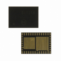
SI1015-A-GM Silicon Laboratories Inc, SI1015-A-GM Datasheet - Page 327

SI1015-A-GM
Manufacturer Part Number
SI1015-A-GM
Description
IC TXRX MCU + EZRADIOPRO
Manufacturer
Silicon Laboratories Inc
Specifications of SI1015-A-GM
Package / Case
42-QFN
Frequency
240MHz ~ 960MHz
Data Rate - Maximum
256kbps
Modulation Or Protocol
FSK, GFSK, OOK
Applications
General Purpose
Power - Output
13dBm
Sensitivity
-121dBm
Voltage - Supply
0.9 V ~ 3.6 V
Current - Receiving
18.5mA
Current - Transmitting
30mA
Data Interface
PCB, Surface Mount
Memory Size
8kB Flash, 768B RAM
Antenna Connector
PCB, Surface Mount
Number Of Receivers
1
Number Of Transmitters
1
Wireless Frequency
240 MHz to 960 MHz
Interface Type
UART, SMBus, SPI, PCA
Output Power
13 dBm
Operating Supply Voltage
0.9 V to 3.6 V
Maximum Operating Temperature
+ 85 C
Mounting Style
SMD/SMT
Maximum Supply Current
4 mA
Minimum Operating Temperature
- 40 C
Modulation
FSK, GFSK, OOK
Protocol Supported
C2, SMBus
Core
8051
Program Memory Type
Flash
Program Memory Size
8 KB
Data Ram Size
768 B
Supply Current (max)
4 mA
Lead Free Status / RoHS Status
Lead free / RoHS Compliant
Operating Temperature
-
Lead Free Status / Rohs Status
Lead free / RoHS Compliant
Other names
336-1868-5
Available stocks
Company
Part Number
Manufacturer
Quantity
Price
Company:
Part Number:
SI1015-A-GM
Manufacturer:
Silicon Labs
Quantity:
135
Part Number:
SI1015-A-GM
Manufacturer:
SILICONLA
Quantity:
20 000
- Current page: 327 of 384
- Download datasheet (3Mb)
operation. Therefore, the SPIF flag serves as both a transmit-complete and receive-data-ready flag. The
data byte received from the slave is transferred MSB-first into the master's shift register. When a byte is
fully shifted into the register, it is moved to the receive buffer where it can be read by the processor by
reading SPI0DAT.
When configured as a master, SPI0 can operate in one of three different modes: multi-master mode, 3-wire
single-master mode, and 4-wire single-master mode. The default, multi-master mode is active when
NSSMD1 (SPI0CN.3) = 0 and NSSMD0 (SPI0CN.2) = 1. In this mode, NSS is an input to the device, and
is used to disable the master SPI0 when another master is accessing the bus. When NSS is pulled low in
this mode, MSTEN (SPI0CN.6) and SPIEN (SPI0CN.0) are set to 0 to disable the SPI master device, and
a Mode Fault is generated (MODF, SPI0CN.5 = 1). Mode Fault will generate an interrupt if enabled. SPI0
must be manually re-enabled in software under these circumstances. In multi-master systems, devices will
typically default to being slave devices while they are not acting as the system master device. In multi-
master mode, slave devices can be addressed individually (if needed) using general-purpose I/O pins.
Figure 26.2 shows a connection diagram between two master devices in multiple-master mode.
3-wire single-master mode is active when NSSMD1 (SPI0CN.3) = 0 and NSSMD0 (SPI0CN.2) = 0. In this
mode, NSS is not used, and is not mapped to an external port pin through the crossbar. Any slave devices
that must be addressed in this mode should be selected using general-purpose I/O pins. Figure 26.3
shows a connection diagram between a master device in 3-wire master mode and a slave device.
4-wire single-master mode is active when NSSMD1 (SPI0CN.3) = 1. In this mode, NSS is configured as an
output pin, and can be used as a slave-select signal for a single SPI device. In this mode, the output value
of NSS is controlled (in software) with the bit NSSMD0 (SPI0CN.2). Additional slave devices can be
addressed using general-purpose I/O pins. Figure 26.4 shows a connection diagram for a master device in
4-wire master mode and two slave devices.
Figure 26.3. 3-Wire Single Master and 3-Wire Single Slave Mode Connection Diagram
Figure 26.2. Multiple-Master Mode Connection Diagram
Device 1
Master
Master
Device
MISO
MOSI
MISO
MOSI
GPIO
NSS
SCK
SCK
Rev. 1.0
GPIO
MISO
MOSI
SCK
NSS
MISO
MOSI
SCK
Device 2
Master
Device
Slave
Si1010/1/2/3/4/5
327
Related parts for SI1015-A-GM
Image
Part Number
Description
Manufacturer
Datasheet
Request
R
Part Number:
Description:
SMD/C°/SINGLE-ENDED OUTPUT SILICON OSCILLATOR
Manufacturer:
Silicon Laboratories Inc
Part Number:
Description:
Manufacturer:
Silicon Laboratories Inc
Datasheet:
Part Number:
Description:
N/A N/A/SI4010 AES KEYFOB DEMO WITH LCD RX
Manufacturer:
Silicon Laboratories Inc
Datasheet:
Part Number:
Description:
N/A N/A/SI4010 SIMPLIFIED KEY FOB DEMO WITH LED RX
Manufacturer:
Silicon Laboratories Inc
Datasheet:
Part Number:
Description:
N/A/-40 TO 85 OC/EZLINK MODULE; F930/4432 HIGH BAND (REV E/B1)
Manufacturer:
Silicon Laboratories Inc
Part Number:
Description:
EZLink Module; F930/4432 Low Band (rev e/B1)
Manufacturer:
Silicon Laboratories Inc
Part Number:
Description:
I°/4460 10 DBM RADIO TEST CARD 434 MHZ
Manufacturer:
Silicon Laboratories Inc
Part Number:
Description:
I°/4461 14 DBM RADIO TEST CARD 868 MHZ
Manufacturer:
Silicon Laboratories Inc
Part Number:
Description:
I°/4463 20 DBM RFSWITCH RADIO TEST CARD 460 MHZ
Manufacturer:
Silicon Laboratories Inc
Part Number:
Description:
I°/4463 20 DBM RADIO TEST CARD 868 MHZ
Manufacturer:
Silicon Laboratories Inc
Part Number:
Description:
I°/4463 27 DBM RADIO TEST CARD 868 MHZ
Manufacturer:
Silicon Laboratories Inc
Part Number:
Description:
I°/4463 SKYWORKS 30 DBM RADIO TEST CARD 915 MHZ
Manufacturer:
Silicon Laboratories Inc
Part Number:
Description:
N/A N/A/-40 TO 85 OC/4463 RFMD 30 DBM RADIO TEST CARD 915 MHZ
Manufacturer:
Silicon Laboratories Inc
Part Number:
Description:
I°/4463 20 DBM RADIO TEST CARD 169 MHZ
Manufacturer:
Silicon Laboratories Inc


