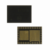
SI1015-A-GM Silicon Laboratories Inc, SI1015-A-GM Datasheet - Page 237

SI1015-A-GM
Manufacturer Part Number
SI1015-A-GM
Description
IC TXRX MCU + EZRADIOPRO
Manufacturer
Silicon Laboratories Inc
Specifications of SI1015-A-GM
Package / Case
42-QFN
Frequency
240MHz ~ 960MHz
Data Rate - Maximum
256kbps
Modulation Or Protocol
FSK, GFSK, OOK
Applications
General Purpose
Power - Output
13dBm
Sensitivity
-121dBm
Voltage - Supply
0.9 V ~ 3.6 V
Current - Receiving
18.5mA
Current - Transmitting
30mA
Data Interface
PCB, Surface Mount
Memory Size
8kB Flash, 768B RAM
Antenna Connector
PCB, Surface Mount
Number Of Receivers
1
Number Of Transmitters
1
Wireless Frequency
240 MHz to 960 MHz
Interface Type
UART, SMBus, SPI, PCA
Output Power
13 dBm
Operating Supply Voltage
0.9 V to 3.6 V
Maximum Operating Temperature
+ 85 C
Mounting Style
SMD/SMT
Maximum Supply Current
4 mA
Minimum Operating Temperature
- 40 C
Modulation
FSK, GFSK, OOK
Protocol Supported
C2, SMBus
Core
8051
Program Memory Type
Flash
Program Memory Size
8 KB
Data Ram Size
768 B
Supply Current (max)
4 mA
Lead Free Status / RoHS Status
Lead free / RoHS Compliant
Operating Temperature
-
Lead Free Status / Rohs Status
Lead free / RoHS Compliant
Other names
336-1868-5
Available stocks
Company
Part Number
Manufacturer
Quantity
Price
Company:
Part Number:
SI1015-A-GM
Manufacturer:
Silicon Labs
Quantity:
135
Part Number:
SI1015-A-GM
Manufacturer:
SILICONLA
Quantity:
20 000
- Current page: 237 of 384
- Download datasheet (3Mb)
SFR Definition 21.17. P1DRV: Port1 Drive Strength
SFR Page = 0xF; SFR Address = 0xA5
SFR Definition 21.18. P2: Port2
SFR Page = All Pages; SFR Address = 0xA0; Bit-Addressable
6:0
Note: P1.0, P1.1, P1.2, and P1.3 are internally connected to the EZRadioPRO peripheral.
Name
Reset
Name
Reset
Type
Bit
Type
7
6:0
Bit
Bit
Bit
7
P1DRV[6:0]
Unused
Name
Unused
Name
R/W
P2
P2
7
0
7
1
Read =0b; Write = Don’t Care.
Drive Strength Configuration Bits for
Configures digital I/O Port cells to high or low output drive strength.
0: Corresponding P1.n Output has low output drive strength.
1: Corresponding P1.n Output has high output drive strength.
Port 2 Data.
Sets the Port latch logic
value or reads the Port pin
logic state in Port cells con-
figured for digital I/O.
Read = 0000000b; Write = Don’t Care.
6
0
6
0
Description
5
0
5
0
Rev. 1.0
4
0
4
0
0: Set output latch to logic
LOW.
1: Set output latch to logic
HIGH.
P1.6–P1.0 (respectively).
P1DRV[6:0]
Function
R/W
Read
3
0
3
0
Si1010/1/2/3/4/5
2
0
2
0
0: P2.7 Port pin is logic
LOW.
1: P2.7 Port pin is logic
HIGH.
1
0
1
0
Write
0
0
0
0
237
Related parts for SI1015-A-GM
Image
Part Number
Description
Manufacturer
Datasheet
Request
R
Part Number:
Description:
SMD/C°/SINGLE-ENDED OUTPUT SILICON OSCILLATOR
Manufacturer:
Silicon Laboratories Inc
Part Number:
Description:
Manufacturer:
Silicon Laboratories Inc
Datasheet:
Part Number:
Description:
N/A N/A/SI4010 AES KEYFOB DEMO WITH LCD RX
Manufacturer:
Silicon Laboratories Inc
Datasheet:
Part Number:
Description:
N/A N/A/SI4010 SIMPLIFIED KEY FOB DEMO WITH LED RX
Manufacturer:
Silicon Laboratories Inc
Datasheet:
Part Number:
Description:
N/A/-40 TO 85 OC/EZLINK MODULE; F930/4432 HIGH BAND (REV E/B1)
Manufacturer:
Silicon Laboratories Inc
Part Number:
Description:
EZLink Module; F930/4432 Low Band (rev e/B1)
Manufacturer:
Silicon Laboratories Inc
Part Number:
Description:
I°/4460 10 DBM RADIO TEST CARD 434 MHZ
Manufacturer:
Silicon Laboratories Inc
Part Number:
Description:
I°/4461 14 DBM RADIO TEST CARD 868 MHZ
Manufacturer:
Silicon Laboratories Inc
Part Number:
Description:
I°/4463 20 DBM RFSWITCH RADIO TEST CARD 460 MHZ
Manufacturer:
Silicon Laboratories Inc
Part Number:
Description:
I°/4463 20 DBM RADIO TEST CARD 868 MHZ
Manufacturer:
Silicon Laboratories Inc
Part Number:
Description:
I°/4463 27 DBM RADIO TEST CARD 868 MHZ
Manufacturer:
Silicon Laboratories Inc
Part Number:
Description:
I°/4463 SKYWORKS 30 DBM RADIO TEST CARD 915 MHZ
Manufacturer:
Silicon Laboratories Inc
Part Number:
Description:
N/A N/A/-40 TO 85 OC/4463 RFMD 30 DBM RADIO TEST CARD 915 MHZ
Manufacturer:
Silicon Laboratories Inc
Part Number:
Description:
I°/4463 20 DBM RADIO TEST CARD 169 MHZ
Manufacturer:
Silicon Laboratories Inc


