SI4313-B1-FM Silicon Laboratories Inc, SI4313-B1-FM Datasheet - Page 28
SI4313-B1-FM
Manufacturer Part Number
SI4313-B1-FM
Description
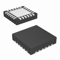
IC RX FSK 315-915MHZ 20VQFN
Manufacturer
Silicon Laboratories Inc
Series
EZRadio®r
Type
ISM Receiverr
Specifications of SI4313-B1-FM
Package / Case
20-VQFN
Mfg Application Notes
Si4313 Register Desc AppNote
Frequency
315MHz, 434MHz, 868MHz, 915MHz
Sensitivity
-118dBm
Data Rate - Maximum
128kbps
Modulation Or Protocol
FSK, GFSK, OOK
Applications
Data Logging, Health Monitors, Remote Control, Weather Station
Data Interface
PCB, Surface Mount
Antenna Connector
PCB, Surface Mount
Voltage - Supply
1.8 V ~ 3.6 V
Operating Temperature
-40°C ~ 85°C
Operating Frequency
315 MHz to 915 MHz
Operating Supply Voltage
1.8 V to 3.6 V
Maximum Operating Temperature
+ 85 C
Minimum Operating Temperature
- 40 C
Mounting Style
SMD/SMT
Supply Current
100 nA
Lead Free Status / RoHS Status
Lead free / RoHS Compliant
Features
-
Memory Size
-
Current - Receiving
-
Lead Free Status / Rohs Status
Lead free / RoHS Compliant
Other names
336-1980-5
Available stocks
Company
Part Number
Manufacturer
Quantity
Price

Company:
Part Number:
SI4313-B1-FMR
Manufacturer:
TI
Quantity:
10 000
Part Number:
SI4313-B1-FMR
Manufacturer:
SILICON LABS/芯科
Quantity:
20 000


Si4313-B1
The typical value of the total on-chip capacitance Cint can be calculated as follows:
Cint = 1.8 pF + 0.085 pF x xlc[6:0] + 3.7 pF x xtalshift
Note that the coarse shift bit xtalshift is not binary with xlc[6:0]. The total load capacitance Cload seen by the crystal
can be calculated by adding the sum of all external parasitic PCB capacitances Cext to Cint. If the maximum value
of Cint (16.3 pF) is not sufficient, an external capacitor can be added for exact tuning. Additional information on
calculating Cext and crystal selection guidelines is provided in “AN417: Si4x3x Family Crystal Oscillator.”
If AFC is disabled then the synthesizer frequency may be further adjusted by programming the Frequency Offset
field fo[9:0]in "Register 73h. Frequency Offset 1" and "Register 74h. Frequency Offset 2", as discussed in "3.5.
Frequency Control" on page 22.
The crystal oscillator frequency is divided down internally and may be output to the microcontroller through one of
the GPIO pins for use as the System Clock. In this fashion, only one crystal oscillator is required for the entire
system and the BOM cost is reduced. The available clock frequencies and GPIO configuration are discussed
further in "8.2. Microcontroller Clock" on page 33.
The Si4313 may also be driven with an external 30 MHz clock signal through the XOUT pin. When driving with an
external reference or using a TCXO, the XTAL load capacitance register should be set to 0.
Add R/W Function/Description
D7
D6
D5
D4
D3
D2
D1
D0
POR Def.
09
R/W
Crystal Oscillator Load
xtalshift
xlc[6]
xlc[5]
xlc[4]
xlc[3]
xlc[2]
xlc[1]
xlc[0]
7Fh
Capacitance
5.8. Regulators
There are a total of six regulators integrated onto the Si4313. With the exception of the digital regulator, all
regulators are designed to operate with only internal decoupling. The digital regulator requires an external 1 µF
decoupling capacitor. All regulators are designed to operate with an input supply voltage from +1.8 to +3.6 V.
A supply voltage should only be connected to the VDD pins. No voltage should be forced on the digital regulator
outputs.
28
Rev. 1.0
Related parts for SI4313-B1-FM
Image
Part Number
Description
Manufacturer
Datasheet
Request
R

Part Number:
Description:
Manufacturer:
Silicon Laboratories Inc
Datasheet:
Part Number:
Description:
SMD/C�/SINGLE-ENDED OUTPUT SILICON OSCILLATOR
Manufacturer:
Silicon Laboratories Inc
Part Number:
Description:
Manufacturer:
Silicon Laboratories Inc
Datasheet:
Part Number:
Description:
N/A N/A/SI4010 AES KEYFOB DEMO WITH LCD RX
Manufacturer:
Silicon Laboratories Inc
Datasheet:
Part Number:
Description:
N/A N/A/SI4010 SIMPLIFIED KEY FOB DEMO WITH LED RX
Manufacturer:
Silicon Laboratories Inc
Datasheet:
Part Number:
Description:
N/A/-40 TO 85 OC/EZLINK MODULE; F930/4432 HIGH BAND (REV E/B1)
Manufacturer:
Silicon Laboratories Inc
Part Number:
Description:
EZLink Module; F930/4432 Low Band (rev e/B1)
Manufacturer:
Silicon Laboratories Inc
Part Number:
Description:
I�/4460 10 DBM RADIO TEST CARD 434 MHZ
Manufacturer:
Silicon Laboratories Inc
Part Number:
Description:
I�/4461 14 DBM RADIO TEST CARD 868 MHZ
Manufacturer:
Silicon Laboratories Inc
Part Number:
Description:
I�/4463 20 DBM RFSWITCH RADIO TEST CARD 460 MHZ
Manufacturer:
Silicon Laboratories Inc
Part Number:
Description:
I�/4463 20 DBM RADIO TEST CARD 868 MHZ
Manufacturer:
Silicon Laboratories Inc
Part Number:
Description:
I�/4463 27 DBM RADIO TEST CARD 868 MHZ
Manufacturer:
Silicon Laboratories Inc
Part Number:
Description:
I�/4463 SKYWORKS 30 DBM RADIO TEST CARD 915 MHZ
Manufacturer:
Silicon Laboratories Inc
Part Number:
Description:
N/A N/A/-40 TO 85 OC/4463 RFMD 30 DBM RADIO TEST CARD 915 MHZ
Manufacturer:
Silicon Laboratories Inc