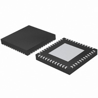
TDA9899HN/V2,551 NXP Semiconductors, TDA9899HN/V2,551 Datasheet - Page 79

TDA9899HN/V2,551
Manufacturer Part Number
TDA9899HN/V2,551
Description
IC IF PROCESSOR MULTISTD 48HVQFN
Manufacturer
NXP Semiconductors
Datasheet
1.TDA9899HLV2151.pdf
(103 pages)
Specifications of TDA9899HN/V2,551
Function
IF Processor
Rf Type
ATV, DVB, FM
Package / Case
48-VFQFN Exposed Pad
Lead Free Status / RoHS Status
Lead free / RoHS Compliant
Other names
935282856551
TDA9899HN/V2-S
TDA9899HN/V2-S
TDA9899HN/V2-S
TDA9899HN/V2-S
- Current page: 79 of 103
- Download datasheet (498Kb)
NXP Semiconductors
Table 58.
V
V
gain controlled amplifier adjusted to typical specified output level; measurements taken in test circuit of
crystal oscillator reference; unless otherwise specified.
TDA9899_3
Product data sheet
Symbol
IF amplifier; pins IF3A and IF3B or IF1A and IF1B or IF2A and IF2B
V
R
C
G
DTV differential output; pins OUT1A, OUT1B, OUT2A and OUT2B
V
I
I
I
R
V
Direct IF; pins OUT2A and OUT2B
G
V
C/N
bias(int)
sink(o)(max)
source(o)(max)
P
i(IF)
IM
I
O
i(IF)(RMS)
o(dif)(p-p)
i(dif)
i(dif)
O
IF(cr)
IF(max)
= 5 V
= 10 mV (RMS); f
[1]
; T
Characteristics
amb
12.2 Digital TV signal processing
= 25 C; 8 MHz system; see
Parameter
input voltage
differential input
resistance
differential input
capacitance
control range IF gain
output voltage
internal bias current
(DC)
maximum output sink
current
maximum output
source current
output resistance
RMS IF input voltage
maximum IF gain
peak-to-peak
differential output
voltage
carrier-to-noise ratio
intermodulation
suppression
IF
= 36 MHz for low IF output of 5 MHz; IF input from 50
Conditions
pin open-circuit
for emitter-follower
DC and AC; see
DC and AC; see
differential; output active
output inactive; internal
resistance to GND
minimum input sine wave
level for nominal output level
maximum input sine wave
level for nominal output level
permissible overload
output peak-to-peak level to
input RMS level ratio
between pin OUT2A and
pin OUT2B
at f
see
input signals: f
and 57.5 MHz; output
signals: f
68.0 MHz; see
W4[7] = 0
W4[7] = 1
V
V
W4[7] = 0
W4[7] = 1
o
i(IF)
i(IF)
Table 36
Figure 38
= 33.4 MHz;
= 10 mV (RMS)
= 0.5 mV (RMS)
Rev. 03 — 15 January 2008
o
= 36.5 MHz or
and
i
Figure 39
= 47.0 MHz
Multistandard hybrid IF processing including car mobile
Figure 37
Figure 37
Table
37; CW test input signal is used for specification;
[2][5][6]
[2]
[2]
[2]
[3]
[3]
[2]
[2]
[2]
[2]
[4]
[2]
Min
1.8
-
-
60
1.8
2.0
1.4
6.0
-
-
-
130
-
-
-
-
115
90
40
40
via broadband transformer 1 : 1;
Typ
1.93
2
3
66
2.0
2.5
1.7
-
-
800
70
170
-
83
1.0
0.50
124
104
-
-
Figure 49
TDA9899
Max
2.2
-
-
-
2.2
-
-
-
50
-
100
-
320
-
1.1
0.55
-
-
-
-
© NXP B.V. 2008. All rights reserved.
with 4 MHz
Unit
V
k
pF
dB
V
mA
mA
mA
mV
mV
dB
V
V
dBc/Hz
dBc/Hz
dB
dB
79 of 103
V
Related parts for TDA9899HN/V2,551
Image
Part Number
Description
Manufacturer
Datasheet
Request
R

Part Number:
Description:
IC IF PROCESSOR MULTISTD 48HVQFN
Manufacturer:
NXP Semiconductors
Datasheet:
Part Number:
Description:
Up-Down Converters MULTI APPL SYS FOR TERRESTR IF
Manufacturer:
NXP Semiconductors
Part Number:
Description:
Up-Down Converters MULTI APPL SYS FOR TERRESTR IF
Manufacturer:
NXP Semiconductors
Part Number:
Description:
Tda9899 Multistandard Hybrid If Processing Including Car Mobile
Manufacturer:
NXP Semiconductors
Datasheet:
Part Number:
Description:
NXP Semiconductors designed the LPC2420/2460 microcontroller around a 16-bit/32-bitARM7TDMI-S CPU core with real-time debug interfaces that include both JTAG andembedded trace
Manufacturer:
NXP Semiconductors
Datasheet:

Part Number:
Description:
NXP Semiconductors designed the LPC2458 microcontroller around a 16-bit/32-bitARM7TDMI-S CPU core with real-time debug interfaces that include both JTAG andembedded trace
Manufacturer:
NXP Semiconductors
Datasheet:
Part Number:
Description:
NXP Semiconductors designed the LPC2468 microcontroller around a 16-bit/32-bitARM7TDMI-S CPU core with real-time debug interfaces that include both JTAG andembedded trace
Manufacturer:
NXP Semiconductors
Datasheet:
Part Number:
Description:
NXP Semiconductors designed the LPC2470 microcontroller, powered by theARM7TDMI-S core, to be a highly integrated microcontroller for a wide range ofapplications that require advanced communications and high quality graphic displays
Manufacturer:
NXP Semiconductors
Datasheet:
Part Number:
Description:
NXP Semiconductors designed the LPC2478 microcontroller, powered by theARM7TDMI-S core, to be a highly integrated microcontroller for a wide range ofapplications that require advanced communications and high quality graphic displays
Manufacturer:
NXP Semiconductors
Datasheet:
Part Number:
Description:
The Philips Semiconductors XA (eXtended Architecture) family of 16-bit single-chip microcontrollers is powerful enough to easily handle the requirements of high performance embedded applications, yet inexpensive enough to compete in the market for hi
Manufacturer:
NXP Semiconductors
Datasheet:
Part Number:
Description:
The XA-S3 device is a member of Philips Semiconductors? XA(eXtended Architecture) family of high performance 16-bitsingle-chip microcontrollers
Manufacturer:
NXP Semiconductors
Datasheet:

Part Number:
Description:
The NXP BlueStreak LH75401/LH75411 family consists of two low-cost 16/32-bit System-on-Chip (SoC) devices
Manufacturer:
NXP Semiconductors
Datasheet:

Part Number:
Description:
The NXP LPC3130/3131 combine an 180 MHz ARM926EJ-S CPU core, high-speed USB2
Manufacturer:
NXP Semiconductors
Datasheet:

Part Number:
Description:
The NXP LPC3141 combine a 270 MHz ARM926EJ-S CPU core, High-speed USB 2
Manufacturer:
NXP Semiconductors


