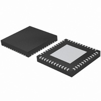
TDA9899HN/V2,551 NXP Semiconductors, TDA9899HN/V2,551 Datasheet - Page 37

TDA9899HN/V2,551
Manufacturer Part Number
TDA9899HN/V2,551
Description
IC IF PROCESSOR MULTISTD 48HVQFN
Manufacturer
NXP Semiconductors
Datasheet
1.TDA9899HLV2151.pdf
(103 pages)
Specifications of TDA9899HN/V2,551
Function
IF Processor
Rf Type
ATV, DVB, FM
Package / Case
48-VFQFN Exposed Pad
Lead Free Status / RoHS Status
Lead free / RoHS Compliant
Other names
935282856551
TDA9899HN/V2-S
TDA9899HN/V2-S
TDA9899HN/V2-S
TDA9899HN/V2-S
- Current page: 37 of 103
- Download datasheet (498Kb)
NXP Semiconductors
Table 55.
V
f
for L); IF input from 50
B/G is 10 % and for L is 3 %; video signal in accordance with “ITU-T J.63 line 17 and line 330” or “NTC-7 Composite”;
internal Nyquist slope switched on (W7[0] = 0); not dual mode; measurements taken in test circuit of
otherwise specified.
TDA9899_3
Product data sheet
Symbol
Power-on reset
V
VIF amplifier; pins IF1A, IF1B, IF2A and IF2B
V
R
C
V
G
f
f
FPLL and true synchronous video demodulator
V
f
f
t
V
SC
VCO(max)
VIF
acq
P
G
f
P(POR)
I
i(IF)(RMS)
3dB(VIF)l
3dB(VIF)u
LFVIF
lock(min)(RMS)
i(dif)
i(dif)
VIF(cr)
VIF(dah)
= 5 V; T
= 32.875 MHz; PC / SC = 13 dB; f
IF
amb
Characteristics
= 25 C; see
Parameter
power-on reset supply
voltage
input voltage
differential input resistance
differential input capacitance
RMS IF input voltage
IF gain variation
control range VIF gain
lower VIF cut-off frequency
upper VIF cut-off frequency
voltage on pin LFVIF (DC)
maximum VCO frequency
VIF frequency
digital acquisition help VIF
frequency window
acquisition time
RMS minimum lock-in
voltage
via broadband transformer 1 : 1; video modulation: Vestigial SideBand (VSB); residual carrier for
Table 26
…continued
for input frequencies; B/G standard is used for the specification (f
AF
= 400 Hz); input level V
Rev. 03 — 15 January 2008
Conditions
for start of reset at
decreasing supply voltage
for end of reset at
increasing supply voltage;
I
enable
lower limit at 1 dB video
output signal
upper limit at +1 dB video
output signal
permissible overload
difference between
picture and sound carrier;
within AGC range;
f
see
related to f
B
measured on pins IF1A
and IF1B or IF2A and
IF2B; maximum IF gain;
negative modulation
mode W2[7] = 1 and PLL
set to overmodulation
mode W2[2] = 0 and
W2[1] = 0
2
VCO
f = 5.5 MHz
C-bus transmission
[5]
LF( 3dB)
all standards except
M/N
M/N standard
Table 26
= 2f
Multistandard hybrid IF processing including car mobile
PC
= 70 kHz
VIF
i(IF)
= 10 mV (RMS) (sync level for B/G; peak white level
[2]
[2]
[3]
[3]
[4]
[6]
Min
2.5
-
-
-
-
-
150
-
-
60
-
-
0.9
120
-
-
-
-
-
Typ
3.0
3.3
1.95
2
3
60
190
-
0.7
66
15
80
-
140
-
-
30
2.3
1.8
Figure
PC
TDA9899
© NXP B.V. 2008. All rights reserved.
= 38.375 MHz;
Max
3.5
4.4
-
-
-
100
-
320
-
-
-
-
3.6
-
-
-
-
30
70
49; unless
Unit
V
V
V
k
pF
mV
mV
dB
dB
MHz
MHz
V
MHz
MHz
MHz
MHz
ms
37 of 103
V
V
Related parts for TDA9899HN/V2,551
Image
Part Number
Description
Manufacturer
Datasheet
Request
R

Part Number:
Description:
IC IF PROCESSOR MULTISTD 48HVQFN
Manufacturer:
NXP Semiconductors
Datasheet:
Part Number:
Description:
Up-Down Converters MULTI APPL SYS FOR TERRESTR IF
Manufacturer:
NXP Semiconductors
Part Number:
Description:
Up-Down Converters MULTI APPL SYS FOR TERRESTR IF
Manufacturer:
NXP Semiconductors
Part Number:
Description:
Tda9899 Multistandard Hybrid If Processing Including Car Mobile
Manufacturer:
NXP Semiconductors
Datasheet:
Part Number:
Description:
NXP Semiconductors designed the LPC2420/2460 microcontroller around a 16-bit/32-bitARM7TDMI-S CPU core with real-time debug interfaces that include both JTAG andembedded trace
Manufacturer:
NXP Semiconductors
Datasheet:

Part Number:
Description:
NXP Semiconductors designed the LPC2458 microcontroller around a 16-bit/32-bitARM7TDMI-S CPU core with real-time debug interfaces that include both JTAG andembedded trace
Manufacturer:
NXP Semiconductors
Datasheet:
Part Number:
Description:
NXP Semiconductors designed the LPC2468 microcontroller around a 16-bit/32-bitARM7TDMI-S CPU core with real-time debug interfaces that include both JTAG andembedded trace
Manufacturer:
NXP Semiconductors
Datasheet:
Part Number:
Description:
NXP Semiconductors designed the LPC2470 microcontroller, powered by theARM7TDMI-S core, to be a highly integrated microcontroller for a wide range ofapplications that require advanced communications and high quality graphic displays
Manufacturer:
NXP Semiconductors
Datasheet:
Part Number:
Description:
NXP Semiconductors designed the LPC2478 microcontroller, powered by theARM7TDMI-S core, to be a highly integrated microcontroller for a wide range ofapplications that require advanced communications and high quality graphic displays
Manufacturer:
NXP Semiconductors
Datasheet:
Part Number:
Description:
The Philips Semiconductors XA (eXtended Architecture) family of 16-bit single-chip microcontrollers is powerful enough to easily handle the requirements of high performance embedded applications, yet inexpensive enough to compete in the market for hi
Manufacturer:
NXP Semiconductors
Datasheet:
Part Number:
Description:
The XA-S3 device is a member of Philips Semiconductors? XA(eXtended Architecture) family of high performance 16-bitsingle-chip microcontrollers
Manufacturer:
NXP Semiconductors
Datasheet:

Part Number:
Description:
The NXP BlueStreak LH75401/LH75411 family consists of two low-cost 16/32-bit System-on-Chip (SoC) devices
Manufacturer:
NXP Semiconductors
Datasheet:

Part Number:
Description:
The NXP LPC3130/3131 combine an 180 MHz ARM926EJ-S CPU core, high-speed USB2
Manufacturer:
NXP Semiconductors
Datasheet:

Part Number:
Description:
The NXP LPC3141 combine a 270 MHz ARM926EJ-S CPU core, High-speed USB 2
Manufacturer:
NXP Semiconductors


