DVK-WLM400 Laird Technologies, DVK-WLM400 Datasheet - Page 11
DVK-WLM400
Manufacturer Part Number
DVK-WLM400
Description
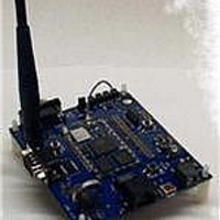
DEVELOPMENT KIT WISM+
Manufacturer
Laird Technologies
Type
Transceiverr
Datasheet
1.DVK-WLM400.pdf
(43 pages)
Specifications of DVK-WLM400
Frequency
2.4GHz
Processor Series
WISM+
Silicon Manufacturer
Laird Technologies
Kit Application Type
Communication & Networking
Application Sub Type
Wi-Fi Intelligent Serial
Kit Contents
PCB, 2x Antennas, Power Adapter, USB Cable, RS-232
Rohs Compliant
Yes
For Use With/related Products
WLM400
Lead Free Status / RoHS Status
Lead free / RoHS Compliant
Lead Free Status / RoHS Status
Lead free / RoHS Compliant, Lead free / RoHS Compliant


2.2.3 I2C Header
This is the WISM+ I2C two-wire interface. It is also connected to the real time clock on the Dev Kit board. These pins
are also compatible with the Ardvark USB to SPI/I2C device, but currently, the only function for the I2C bus is the
interface to the Real-Time-Clock populated on the Dev Kit PCB. In the future, this interface might be set up so the
WISM+ can interface to other defined I2C sensors.
2.2.4 10/100 Ethernet Connector
This is a standard RJ-45 Ethernet connector and is another host interface to the WISM+. A standard Ethernet cable
can be connected between a PC and the Dev Kit and WIF.exe can be configured to operate over the PC’s Ethernet
port.
2.2.5 USB Device “MINI” Connector
This is a standard USB mini connector which can be used to connect the Dev Kit to a PC over the host USB interface.
A USB cable is provided to connect to a PC. By default, WIF.exe will use the USB port for WISM+ communications.
This is the recommended interface to use for the Dev Kit right out of the box.
On the Dev Kit PCB, the USB connector is wired to the WISM+ USB device pins: WISM+ pin 4 (USB_DDM) and
WISM+ pin 5 (USB_DDP).
2.2.6 Debug Com Port
This is an RS-232 DCE serial port. This port outputs internal debug information which can be used by Laird
Technologies to attempt to debug WISM+ operations. There is no hardware flow control. DB9 Pin 2 is transmit data to
the PC, and DB9 pin 3 is receive data from the PC.
2.3 RF
2.3.1 WISM+ U.FL Port#1 & #2
These are the two WISM+ RF ports. They utilize a miniature U.FL type non-standard RF connector per FCC/IC rules.
The WISM+ Dev Kit comes with two antennae connected. This gives you the ability to test antenna diversity, or to
configure a single antenna.
NOTE: See section: “
antenna configuration.
2.3.2 Antenna Mounting Holes
These holes are used to mount antennae. Both mounting holes can have antennae installed and connected to WISM+
RF ports #1 & #2 U.FL connectors. The Dev Kit is shipped stock with both antennae and is configured out of the box
to use antenna diversity.
© Laird Technology 2010
I2C Header
4,5,6,7,8,9
PIN#
2,10
1
3
I2C Header
I2C_CLK
I2C_DAT
GND
N/C
PIN NAME
Configure WISM+ Antenna
I/O
I/O
I/O
WISM+
PIN #
23
22
PIN NAME
I2C_CLK
I2C_DAT
WISM+
” for the details on the procedure to change the WISM+
DESCRIPTION
This is the I2C clock line.
This is the I2C data line.
These pins are tied to the ground plane of the
Dev Kit PCB
These pins are not connected.
Version 1.00
WISM+ DVK MANUAL
Page 6
Related parts for DVK-WLM400
Image
Part Number
Description
Manufacturer
Datasheet
Request
R

Part Number:
Description:
BLUETOOTH EVAL BOARD BTM511
Manufacturer:
Laird Technologies
Datasheet:

Part Number:
Description:
Bluetooth / 802.15.1 Modules & Development Tools BLUETTH AT Data MODLE, No ANT DEVKIT
Manufacturer:
Laird Technologies
Part Number:
Description:
Bluetooth / 802.15.1 Modules & Development Tools BLUETTH Multimed MODLE, No ANT DEVKIT
Manufacturer:
Laird Technologies
Datasheet:

Part Number:
Description:
BLUETOOTH MODULE DEVELOPMENT KIT
Manufacturer:
Laird Technologies
Part Number:
Description:
Bluetooth 2.0 AT Data Module, Internal Antenna Development Kit
Manufacturer:
Laird Technologies

Part Number:
Description:
BT MM DEV KIT
Manufacturer:
Laird Technologies
Datasheet:
Part Number:
Description:
Bluetooth / 802.15.1 Modules & Development Tools BLUETTH HCI Data MDLE INTRNLANT DVKIT
Manufacturer:
Laird Technologies
Datasheet:
Part Number:
Description:
Bluetooth / 802.15.1 Modules & Development Tools BLUETTHMultimedMODLE Plus No Ant DEVKIT
Manufacturer:
Laird Technologies
Part Number:
Description:
Bluetooth / 802.15.1 Modules & Development Tools BLUETTH HCI Data MDLE No ANT DVKIT
Manufacturer:
Laird Technologies
Datasheet:

Part Number:
Description:
KIT FOR PRM113
Manufacturer:
Laird Technologies
Datasheet:

Part Number:
Description:
DEV KIT PRM122
Manufacturer:
Laird Technologies
Datasheet:
Part Number:
Description:
DEV KIT PRM123
Manufacturer:
Laird Technologies
Datasheet:

Part Number:
Description:
KIT FOR PRM112
Manufacturer:
Laird Technologies
Datasheet:
Part Number:
Description:
DEV KIT PRM121
Manufacturer:
Laird Technologies
Datasheet:

Part Number:
Description:
Bluetooth / 802.15.1 Modules Class2 v2.1+EDR Kit AT Data, Int Ant,SSP
Manufacturer:
Laird Technologies Wireless M2M
Datasheet: