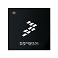
XC56309VL100A Freescale Semiconductor, XC56309VL100A Datasheet - Page 22

XC56309VL100A
Manufacturer Part Number
XC56309VL100A
Description
IC DSP 24BIT 100MHZ 196-MAPBGA
Manufacturer
Freescale Semiconductor
Series
DSP563xxr
Type
Fixed Pointr
Specifications of XC56309VL100A
Interface
Host Interface, SSI, SCI
Clock Rate
100MHz
Non-volatile Memory
ROM (576 B)
On-chip Ram
24kB
Voltage - I/o
3.30V
Voltage - Core
3.30V
Operating Temperature
-40°C ~ 100°C
Mounting Type
Surface Mount
Package / Case
196-MAPBGA
Device Core Size
24b
Format
Fixed Point
Clock Freq (max)
100MHz
Mips
100
Device Input Clock Speed
100MHz
Ram Size
102KB
Operating Supply Voltage (typ)
3.3V
Operating Supply Voltage (min)
3V
Operating Supply Voltage (max)
3.6V
Operating Temp Range
-40C to 100C
Operating Temperature Classification
Industrial
Mounting
Surface Mount
Pin Count
196
Package Type
MA-BGA
Lead Free Status / RoHS Status
Lead free / RoHS Compliant
Available stocks
Company
Part Number
Manufacturer
Quantity
Price
Company:
Part Number:
XC56309VL100A
Manufacturer:
Freescale Semiconductor
Quantity:
10 000
Company:
Part Number:
XC56309VL100AR2
Manufacturer:
Freescale Semiconductor
Quantity:
10 000
- Current page: 22 of 284
- Download datasheet (4Mb)
DSP56309 Overview
1.9 Peripherals
In addition to the core features, the DSP56309 provides the following peripherals:
1.9.1 GPIO Functionality
The GPIO port consists of up to 34 programmable signals, also used by the peripherals (HI08,
ESSI, SCI, and timer). There are no dedicated GPIO signals. After a reset, the signals are
automatically configured as GPIO. Three memory-mapped registers per peripheral control GPIO
functionality. Programming techniques for these registers to control GPIO functionality are
detailed in Chapter 5, Programming the Peripherals.
1.9.2 HI08
The HI08 is a byte-wide, full-duplex, double-buffered parallel port that can connect directly to
the data bus of a host processor. The HI08 supports a variety of buses and provides connection
with a number of industry-standard DSPs, microcomputers, and microprocessors without
requiring any additional logic. The DSP core treats the HI08 as a memory-mapped peripheral
occupying eight 24-bit words in data memory space. The DSP can use the HI08 as a
memory-mapped peripheral, using either standard polled or interrupt programming techniques.
Separate double-buffered transmit and receive data registers allow the DSP and host processor to
transfer data efficiently at high speed. Memory mapping allows you to program DSP core
communication with the HI08 registers using standard instructions and addressing modes.
1.9.3 ESSI
The DSP56309 provides two independent and identical ESSIs. Each ESSI has a full-duplex serial
port for communication with a variety of serial devices, including one or more industry-standard
codecs, other DSPs, microprocessors, and peripherals that implement the Freescale SPI. The
ESSI consists of independent transmitter and receiver sections and a common ESSI clock
generator. ESSI capabilities include the following:
1-12
As many as 34 user-configurable GPIO signals
HI08 to external hosts
Dual ESSI
SCI
Triple timer module
Memory switch mode
Four external interrupt/mode control lines
Independent (asynchronous) or shared (synchronous) transmit and receive sections with
separate or shared internal/external clocks and frame syncs
Normal mode operation using frame sync
DSP56309 User’s Manual, Rev. 1
Freescale Semiconductor
Related parts for XC56309VL100A
Image
Part Number
Description
Manufacturer
Datasheet
Request
R
Part Number:
Description:
Manufacturer:
Freescale Semiconductor, Inc
Datasheet:
Part Number:
Description:
Manufacturer:
Freescale Semiconductor, Inc
Datasheet:
Part Number:
Description:
Manufacturer:
Freescale Semiconductor, Inc
Datasheet:
Part Number:
Description:
Manufacturer:
Freescale Semiconductor, Inc
Datasheet:
Part Number:
Description:
Manufacturer:
Freescale Semiconductor, Inc
Datasheet:
Part Number:
Description:
Manufacturer:
Freescale Semiconductor, Inc
Datasheet:
Part Number:
Description:
Manufacturer:
Freescale Semiconductor, Inc
Datasheet:
Part Number:
Description:
Manufacturer:
Freescale Semiconductor, Inc
Datasheet:
Part Number:
Description:
Manufacturer:
Freescale Semiconductor, Inc
Datasheet:
Part Number:
Description:
Manufacturer:
Freescale Semiconductor, Inc
Datasheet:
Part Number:
Description:
Manufacturer:
Freescale Semiconductor, Inc
Datasheet:
Part Number:
Description:
Manufacturer:
Freescale Semiconductor, Inc
Datasheet:
Part Number:
Description:
Manufacturer:
Freescale Semiconductor, Inc
Datasheet:
Part Number:
Description:
Manufacturer:
Freescale Semiconductor, Inc
Datasheet:
Part Number:
Description:
Manufacturer:
Freescale Semiconductor, Inc
Datasheet:


