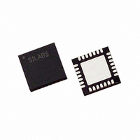
C8051F311 Silicon Laboratories Inc, C8051F311 Datasheet - Page 51

C8051F311
Manufacturer Part Number
C8051F311
Description
IC 8051 MCU 16K FLASH 28MLP
Manufacturer
Silicon Laboratories Inc
Series
C8051F31xr
Specifications of C8051F311
Core Processor
8051
Core Size
8-Bit
Speed
25MHz
Connectivity
SMBus (2-Wire/I²C), SPI, UART/USART
Peripherals
POR, PWM, Temp Sensor, WDT
Number Of I /o
25
Program Memory Size
16KB (16K x 8)
Program Memory Type
FLASH
Ram Size
1.25K x 8
Voltage - Supply (vcc/vdd)
2.7 V ~ 3.6 V
Data Converters
A/D 17x10b
Oscillator Type
Internal
Operating Temperature
-40°C ~ 85°C
Package / Case
28-VQFN Exposed Pad, 28-HVQFN, 28-SQFN, 28-DHVQFN
Lead Free Status / RoHS Status
Contains lead / RoHS non-compliant
Eeprom Size
-
Available stocks
Company
Part Number
Manufacturer
Quantity
Price
Part Number:
C8051F311-GM
Manufacturer:
SILICONLABS/芯科
Quantity:
20 000
Part Number:
C8051F311-GMR
Manufacturer:
SILICON LABS/芯科
Quantity:
20 000
5.
The ADC0 subsystem for the C8051F310/1/2/3/6 consists of two analog multiplexers (referred to collec-
tively as AMUX0) with 25 total input selections, and a 200 ksps, 10-bit successive-approximation-register
ADC with integrated track-and-hold and programmable window detector. The AMUX0, data conversion
modes, and window detector are all configurable under software control via the Special Function Registers
shown in Figure 5.1. ADC0 operates in both Single-ended and Differential modes, and may be configured
to measure P1.0–P3.4, the Temperature Sensor output, or V
The ADC0 subsystem is enabled only when the AD0EN bit in the ADC0 Control register (ADC0CN) is set
to logic 1. The ADC0 subsystem is in low power shutdown when this bit is logic 0.
5.1.
AMUX0 selects the positive and negative inputs to the ADC. Any of the following may be selected as the
positive input: P1.0-P3.4, the on-chip temperature sensor, or the positive power supply (V
following may be selected as the negative input: P1.0-P3.4, VREF, or GND. When GND is selected as
the negative input, ADC0 operates in Single-ended Mode; all other times, ADC0 operates in Differ-
ential Mode. The ADC0 input channels are selected in the AMX0P and AMX0N registers as described in
SFR Definition 5.1 and SFR Definition 5.2.
The conversion code format differs between Single-ended and Differential modes. The registers ADC0H
and ADC0L contain the high and low bytes of the output conversion code from the ADC at the completion
of each conversion. Data can be right-justified or left-justified, depending on the setting of the AD0LJST bit
(ADC0CN.0). When in Single-ended Mode, conversion codes are represented as 10-bit unsigned integers.
P2.6-2.7 available on
C8051F310/1/2/3/4/5
P2.6-2.7 available on
C8051F310/1/2/3/4/5
P1.6-1.7 available on
C8051F310/1/2/3/4/5
P1.6-1.7 available on
C8051F310/1/2/3/4/5
C8051F310/2
C8051F310/2
10-Bit ADC (ADC0, C8051F310/1/2/3/6 only)
available on
available on
Analog Multiplexer
P3.1-3.4
P3.1-3.4
Sensor
Temp
VREF
GND
VDD
P1.0
P1.7
P2.0
P2.7
P3.0
P3.4
P1.0
P1.7
P2.0
P2.7
P3.0
P3.4
Figure 5.1. ADC0 Functional Block Diagram
23-to-1
23-to-1
AMUX
AMUX
AMX0P
AMX0N
Rev. 1.7
C8051F310/1/2/3/4/5/6/7
DD
(+)
(-)
ADC0CF
with respect to P1.0–P3.4, VREF, or GND.
ADC
10-Bit
VDD
SAR
ADC0GTH ADC0GTL
ADC0LTH
ADC0CN
ADC0LTL
Conversion
Start
100
000
001
010
011
101
DD
32
). Any of the
AD0WINT
Compare
Window
AD0BUSY (W)
Timer 0 Overflow
Timer 2 Overflow
Timer 1 Overflow
CNVSTR Input
Timer 3 Overflow
Logic
51


