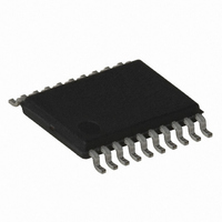
ATTINY167-15XZ Atmel, ATTINY167-15XZ Datasheet - Page 205

ATTINY167-15XZ
Manufacturer Part Number
ATTINY167-15XZ
Description
MCU AVR 16K FLASH 15MHZ 20-TSSOP
Manufacturer
Atmel
Series
AVR® ATtinyr
Datasheet
1.ATTINY167-15MD.pdf
(283 pages)
Specifications of ATTINY167-15XZ
Core Processor
AVR
Core Size
8-Bit
Speed
16MHz
Connectivity
I²C, LIN, SPI, UART/USART, USI
Peripherals
Brown-out Detect/Reset, POR, PWM, Temp Sensor, WDT
Number Of I /o
16
Program Memory Size
16KB (8K x 16)
Program Memory Type
FLASH
Eeprom Size
512 x 8
Ram Size
512 x 8
Voltage - Supply (vcc/vdd)
2.7 V ~ 5.5 V
Data Converters
A/D 11x10b
Oscillator Type
Internal
Operating Temperature
-40°C ~ 125°C
Package / Case
20-TSSOP
For Use With
ATSTK600-SOIC - STK600 SOCKET/ADAPTER FOR SOIC
Lead Free Status / RoHS Status
Lead free / RoHS Compliant
- Current page: 205 of 283
- Download datasheet (5Mb)
17.11 Register Description
17.11.1
7728G–AVR–06/10
ADMUX – ADC Multiplexer Selection Register
• Bit 7:6 – REFS1:REFS0: Voltage Reference Selection Bits
These bits and AREFEN bit from the Analog Miscellaneous Control Register (AMISCR) select
the voltage reference for the ADC, as shown in
conversion, the change will not go in effect until this conversion is complete (ADIF in ADCSRA
register is set). Whenever these bits are changed, the next conversion will take 25 ADC clock
cycles. If active channels are used, using AVCC or an external AREF higher than (AVcc - 1V)
is not recommended, as this will affect ADC accuracy. The internal voltage reference options
may not be used if an external voltage is being applied to the AREF pin.
Table 17-4.
• Bit 5 – ADLAR: ADC Left Adjust Result
The ADLAR bit affects the presentation of the ADC conversion result in the ADC Data Regis-
ter. Write one to ADLAR to left adjust the result. Otherwise, the result is right adjusted.
Changing the ADLAR bit will affect the ADC Data Register immediately, regardless of any
ongoing conversions. For a complete description of this bit, see
Data Register” on page
• Bits 4:0 – MUX4:0: Analog Channel and Gain Selection Bits
These bits select which combination of analog inputs are connected to the ADC. In case of dif-
ferential input, gain selection is also made with these bits. Refer to
these bits are changed during a conversion, the change will not go into effect until this
conversion is complete (ADIF in ADCSRA register is set).
Bit
Read/Write
Initial Value
REFS1
X
X
0
1
REFS0
Voltage Reference Selections for ADC
REFS1
0
0
1
1
R/W
7
0
AREFEN Voltage Reference (V
REFS0
208.
R/W
6
0
0
1
0
0
ADLAR
AVcc used as Voltage Reference, diconnected from AREF pin.
External Voltage Reference at AREF pin (AREF
Internal 1.1V Voltage Reference .
Internal 2.56V Voltage Reference .
R/W
5
0
MUX4
R/W
4
0
Table
MUX3
R/W
3
0
REF
17-4. If these bits are changed during a
) Selection
ATtiny87/ATtiny167
MUX2
R/W
2
0
“ADCL and ADCH – The ADC
MUX1
R/W
Table 17-5
1
0
MUX0
R/W
2.0V)
0
0
for details. If
ADMUX
205
Related parts for ATTINY167-15XZ
Image
Part Number
Description
Manufacturer
Datasheet
Request
R

Part Number:
Description:
Manufacturer:
Atmel Corporation
Datasheet:

Part Number:
Description:
Manufacturer:
Atmel Corporation
Datasheet:

Part Number:
Description:
MCU AVR 16K FLASH 15MHZ 32-QFN
Manufacturer:
Atmel
Datasheet:

Part Number:
Description:
IC MCU AVR 16K FLASH 20TSSOP
Manufacturer:
Atmel
Datasheet:

Part Number:
Description:
MCU AVR 16K FLASH 15MHZ 32-QFN
Manufacturer:
Atmel
Datasheet:

Part Number:
Description:
MCU AVR 16K FLASH 15MHZ 20-SOIC
Manufacturer:
Atmel
Datasheet:

Part Number:
Description:
MCU AVR 16K FLASH 15MHZ 20-TSSOP
Manufacturer:
Atmel
Datasheet:

Part Number:
Description:
IC MCU AVR 16K FLASH 20SOIC
Manufacturer:
Atmel
Datasheet:


