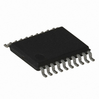
ATTINY167-15XZ Atmel, ATTINY167-15XZ Datasheet - Page 132

ATTINY167-15XZ
Manufacturer Part Number
ATTINY167-15XZ
Description
MCU AVR 16K FLASH 15MHZ 20-TSSOP
Manufacturer
Atmel
Series
AVR® ATtinyr
Datasheet
1.ATTINY167-15MD.pdf
(283 pages)
Specifications of ATTINY167-15XZ
Core Processor
AVR
Core Size
8-Bit
Speed
16MHz
Connectivity
I²C, LIN, SPI, UART/USART, USI
Peripherals
Brown-out Detect/Reset, POR, PWM, Temp Sensor, WDT
Number Of I /o
16
Program Memory Size
16KB (8K x 16)
Program Memory Type
FLASH
Eeprom Size
512 x 8
Ram Size
512 x 8
Voltage - Supply (vcc/vdd)
2.7 V ~ 5.5 V
Data Converters
A/D 11x10b
Oscillator Type
Internal
Operating Temperature
-40°C ~ 125°C
Package / Case
20-TSSOP
For Use With
ATSTK600-SOIC - STK600 SOCKET/ADAPTER FOR SOIC
Lead Free Status / RoHS Status
Lead free / RoHS Compliant
- Current page: 132 of 283
- Download datasheet (5Mb)
12.11 16-bit Timer/Counter Register Description
12.11.1
132
ATtiny87/ATtiny167
Timer/Counter1 Control Register A – TCCR1A
Figure 12-14. Timer/Counter Timing Diagram, with Prescaler (f
• Bit 7:6 – COM1A1:0: Compare Output Mode for Channel A
• Bit 5:4 – COM1B1:0: Compare Output Mode for Channel B
The COM1A1:0 and COM1B1:0 control the Output Compare pins (OC1Ai and OC1Bi respec-
tively) behavior. If one or both of the COM1A1:0 bits are written to one, the OC1Ai output
overrides the normal port functionality of the I/O pin it is connected to. If one or both of the
COM1B1:0 bit are written to one, the OC1Bi output overrides the normal port functionality of
the I/O pin it is connected to. However, note that the Data Direction Register (DDR) bit and
OC1xi bit (TCCR1D) corresponding to the OC1Ai or OC1Bi pin must be set in order to enable
the output driver.
When the OC1Ai or OC1Bi is connected to the pin, the function of the COM1A/B1:0 bits is
dependent of the WGM13:0 bits setting.
when the WGM13:0 bits are set to a Normal or a CTC mode (non-PWM).
Table 12-1.
Bit
Read/Write
Initial Value
OC1Ai
OC1Bi
0
1
and ICF n
(PC and PFC PWM)
TOVn
(CTC and FPWM)
(Update at TOP)
COM1A1
COM1B1
TCNTn
TCNTn
as TOP)
(clk
clk
OCRnx
clk
COM1A1
I/O
(FPWM)
I/O
Tn
/8)
Compare Output Mode, non-PWM
R/W
(if used
x
0
0
1
1
7
0
COM1A0
R/W
COM1A0
COM1B0
6
0
x
0
1
0
1
TOP - 1
TOP - 1
Old OCRnx Value
COM1B1
R/W
5
0
Description
Normal port operation, OC1A/OC1B disconnected.
Toggle OC1A/OC1B on Compare Match.
Clear OC1A/OC1B on Compare Match (Set output to low
level).
Set OC1A/OC1B on Compare Match (Set output to high level).
COM1B0
Table 12-1
R/W
4
0
TOP
TOP
R
3
–
0
shows the COM1A/B1:0 bit functionality
BOTTOM
TOP - 1
–
R
2
0
clk_I/O
New OCRnx Value
/8)
WGM11
R/W
1
0
BOTTOM + 1
TOP - 2
WGM10
R/W
7728G–AVR–06/10
0
0
TCCR1A
Related parts for ATTINY167-15XZ
Image
Part Number
Description
Manufacturer
Datasheet
Request
R

Part Number:
Description:
Manufacturer:
Atmel Corporation
Datasheet:

Part Number:
Description:
Manufacturer:
Atmel Corporation
Datasheet:

Part Number:
Description:
MCU AVR 16K FLASH 15MHZ 32-QFN
Manufacturer:
Atmel
Datasheet:

Part Number:
Description:
IC MCU AVR 16K FLASH 20TSSOP
Manufacturer:
Atmel
Datasheet:

Part Number:
Description:
MCU AVR 16K FLASH 15MHZ 32-QFN
Manufacturer:
Atmel
Datasheet:

Part Number:
Description:
MCU AVR 16K FLASH 15MHZ 20-SOIC
Manufacturer:
Atmel
Datasheet:

Part Number:
Description:
MCU AVR 16K FLASH 15MHZ 20-TSSOP
Manufacturer:
Atmel
Datasheet:

Part Number:
Description:
IC MCU AVR 16K FLASH 20SOIC
Manufacturer:
Atmel
Datasheet:


