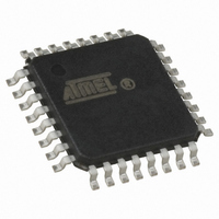
AT90S2333-8AC Atmel, AT90S2333-8AC Datasheet - Page 80

AT90S2333-8AC
Manufacturer Part Number
AT90S2333-8AC
Description
IC MCU 2K FLSH 8MHZ A/D 32TQFP
Manufacturer
Atmel
Series
AVR® 90Sr
Datasheet
1.AT90LS2333-4AC.pdf
(103 pages)
Specifications of AT90S2333-8AC
Core Processor
AVR
Core Size
8-Bit
Speed
8MHz
Connectivity
SPI, UART/USART
Peripherals
Brown-out Detect/Reset, POR, PWM, WDT
Number Of I /o
20
Program Memory Size
2KB (1K x 16)
Program Memory Type
FLASH
Eeprom Size
128 x 8
Ram Size
128 x 8
Voltage - Supply (vcc/vdd)
4 V ~ 6 V
Data Converters
A/D 6x10b
Oscillator Type
Internal
Operating Temperature
0°C ~ 70°C
Package / Case
32-TQFP, 32-VQFP
Lead Free Status / RoHS Status
Contains lead / RoHS non-compliant
- Current page: 80 of 103
- Download datasheet (2Mb)
Data Polling EEPROM
When a byte is being programmed into the EEPROM, reading the address location being programmed will give the value
P1 until the auto-erase is finished, and then the value P2. See Table 34 for P1 and P2 values.
At the time the device is ready for a new EEPROM byte, the programmed value will read correctly. This is used to deter-
mine when the next byte can be written. This will not work for the values P1 and P2, so when programming these values,
the user will have to wait for at least the prescribed time
t
$FF, can be skipped. This does not apply if the EEPROM is reprogrammed without first chip-erasing the device.
Table 34. Read Back Value during EEPROM polling
Data Polling Flash
When a byte is being programmed into the Flash, reading the address location being programmed will give the value $FF.
At the time the device is ready for a new byte, the programmed value will read correctly. This is used to determine when the
next byte can be written. This will not work for the value $FF, so when programming this value, the user will have to wait for
at least t
addresses that are meant to contain $FF, can be skipped.
Figure 67. Serial Programming Waveforms
80
WD_PROG
Part
AT90S/LS2333
AT90S/LS4433
SERIAL DATA OUTPUT
value. As a chip-erased device contains $FF in all locations, programming of addresses that are meant to contain
WD_PROG
SERIAL CLOCK INPUT
SERIAL DATA INPUT
AT90S/LS2333 and AT90S/LS4433
before programming the next byte. As a chip-erased device contains $FF in all locations, programming of
PB3(MOSI)
PB4(MISO)
PB5(SCK)
MSB
MSB
P1
$00
$00
t
WD_PROG
before programming the next byte. See Table 38 for
P2
$FF
$FF
LSB
LSB
Related parts for AT90S2333-8AC
Image
Part Number
Description
Manufacturer
Datasheet
Request
R

Part Number:
Description:
DEV KIT FOR AVR/AVR32
Manufacturer:
Atmel
Datasheet:

Part Number:
Description:
INTERVAL AND WIPE/WASH WIPER CONTROL IC WITH DELAY
Manufacturer:
ATMEL Corporation
Datasheet:

Part Number:
Description:
Low-Voltage Voice-Switched IC for Hands-Free Operation
Manufacturer:
ATMEL Corporation
Datasheet:

Part Number:
Description:
MONOLITHIC INTEGRATED FEATUREPHONE CIRCUIT
Manufacturer:
ATMEL Corporation
Datasheet:

Part Number:
Description:
AM-FM Receiver IC U4255BM-M
Manufacturer:
ATMEL Corporation
Datasheet:

Part Number:
Description:
Monolithic Integrated Feature Phone Circuit
Manufacturer:
ATMEL Corporation
Datasheet:

Part Number:
Description:
Multistandard Video-IF and Quasi Parallel Sound Processing
Manufacturer:
ATMEL Corporation
Datasheet:

Part Number:
Description:
High-performance EE PLD
Manufacturer:
ATMEL Corporation
Datasheet:

Part Number:
Description:
8-bit Flash Microcontroller
Manufacturer:
ATMEL Corporation
Datasheet:

Part Number:
Description:
2-Wire Serial EEPROM
Manufacturer:
ATMEL Corporation
Datasheet:


